Shutdown, Click-and-pop suppression, Applications information – Rainbow Electronics MAX98314 User Manual
Page 11: Filterless class d operation, Speaker amplifier power-supply input (pvdd), Layout and grounding, Figure 2. low-frequency thd+n performance
���������������������������������������������������������������� Maxim Integrated Products 11
MAX98314
Mono 3.2W Class D Amplifier
with Integrated Input Coupling Capacitors
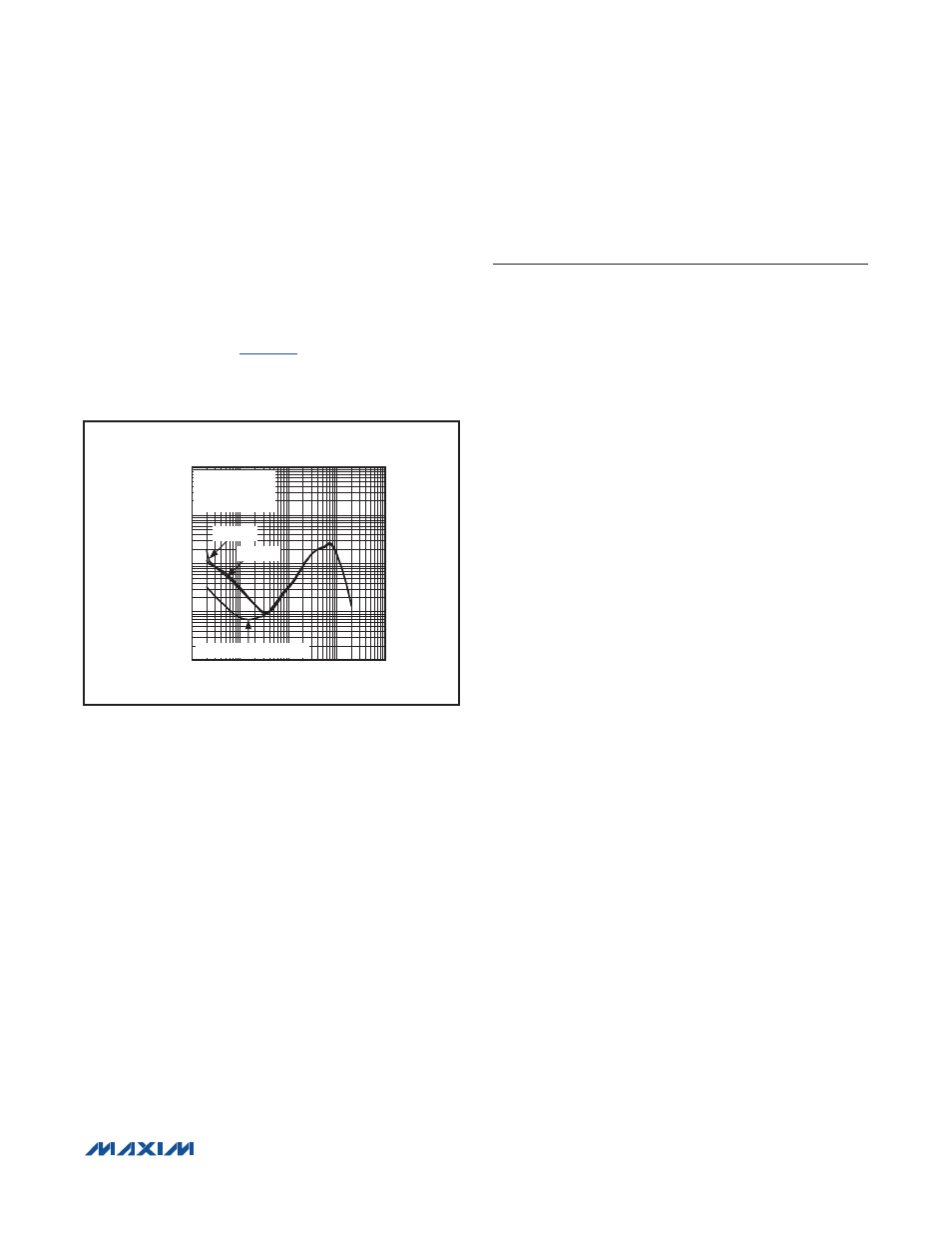
Assuming zero source impedance, the -3dB corner
frequency, f
-3dB
, is:
f
-3dB
= 1/2GR
IN
C
IN
[Hz]
The 100ppm/V voltage coefficient of the integrated input
coupling capacitor results in excellent low-frequency
THD+N performance.
illustrates the superior
linearity of the IC’s integrated input coupling capacitors
compared to a similar amplifier with external 0.01FF X7R
and X5R 0402 input coupling capacitors.
Shutdown
The IC features a low-power shutdown mode, drawing
< 0.1FA (typ) of supply current. Drive SHDN low to put
the IC into shutdown.
Click-and-Pop Suppression
The speaker amplifier features Maxim’s comprehensive
click-and-pop suppression. During startup, the click-
and-pop suppression circuitry reduces any audible
transient sources internal to the device. When entering
shutdown, the differential speaker outputs ramp down to
PGND quickly and simultaneously.
Applications Information
Filterless Class D Operation
Traditional Class D amplifiers require an output filter.
The filter adds cost and size, and decreases efficiency
and THD+N performance. The IC’s filterless modulation
scheme does not require an output filter.
Because the switching frequency of the IC is well beyond
the bandwidth of most speakers, voice coil movement
due to the switching frequency is very small. Use a
speaker with a series inductance > 10FH. Typical 8I
speakers exhibit series inductances in the 20FH to
100FH range.
Speaker Amplifier Power-Supply Input (PVDD)
PVDD powers the speaker amplifier and ranges from
2.5V to 5.5V. Bypass PVDD with a 0.1FF and 10FF
capacitor to PGND. Apply additional bulk capacitance
at the device if long input traces between PVDD and the
power source are used.
Layout and Grounding
Proper layout and grounding are essential for optimum
performance. Good grounding improves audio perfor-
mance and prevents switching noise from coupling into
the audio signal.
Use wide, low-resistance output traces. As the load
impedance decreases, the current drawn from the
device increases. At higher current, the resistance of the
output traces decrease the power delivered to the load.
For example, if 2W is delivered from the device output to
a 4I load through 100mI of total speaker trace, 1.904W
is delivered to the speaker. If power is delivered through
10mI of total speaker trace, 1.99W is delivered to the
speaker. Wide output, supply, and ground traces also
improve the power dissipation of the device.
The IC is inherently designed for excellent RF immunity.
For best performance, add ground fills around all signal
traces on top or bottom PCB layers.
Figure 2. Low-Frequency THD+N Performance
TOTAL HARMONIC DISTORTION
PLUS NOISE vs. FREQUENCY
FREQUENCY (Hz)
THD+N (%)
10k
1k
100
0.01
0.1
1.0
10
0.001
10
100k
V
PVDD
= 4.2V
Z
LOAD
= 8I + 68µH
P
OUT
= 600mW
MAX98314 INTERNAL CAPS
X7R CAPS
X5R CAPS