Absolute maximum ratings, Electrical characteristics – Rainbow Electronics MAX13486E User Manual
Page 2
MAX13485E/MAX13486E
Half-Duplex RS-485/RS-422 Transceivers in µDFN
2
_______________________________________________________________________________________
ABSOLUTE MAXIMUM RATINGS
Stresses beyond those listed under “Absolute Maximum Ratings” may cause permanent damage to the device. These are stress ratings only, and functional
operation of the device at these or any other conditions beyond those indicated in the operational sections of the specifications is not implied. Exposure to
absolute maximum rating conditions for extended periods may affect device reliability.
(All voltages referenced to GND.)
V
CC
........................................................................................+6V
DE,
RE, DI.................................................................-0.3V to +6V
A, B ..............................................................................-8V to 13V
Short-Circuit Duration (RO, A, B) to GND ..................Continuous
Continuous Power Dissipation (T
A
= +70°C)
8-Pin SO (derate 5.9mW/°C above +70°C)..................471mW
8-Pin µDFN (derate 4.8mW/°C above +70°C) ..........380.6mW
Operating Temperature Range ...........................-40°C to +85°C
Junction Temperature ......................................................+150°C
Storage Temperature Range .............................-65°C to +150°C
Lead Temperature (soldering, 10s) .................................+300°C
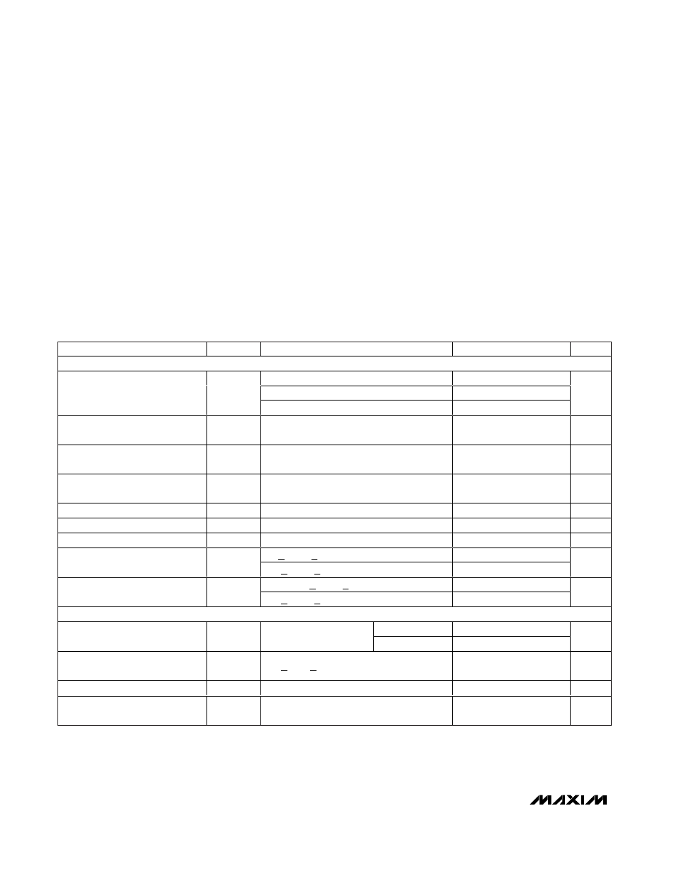
ELECTRICAL CHARACTERISTICS
(V
CC
= +5V ±5%, T
A
= T
MIN
to T
MAX
, unless otherwise noted. Typical values are at V
CC
= +5V and T
A
= +25°C.) (Notes 1, 2)
PARAMETER
SYMBOL
CONDITIONS
MIN
TYP
MAX
UNITS
DRIVER
R
DIFF
= 100
Ω, Figure 1
2.0
V
CC
R
DIFF
= 54
Ω, Figure 1
1.5
Differential Driver Output
V
OD
No load
V
CC
V
Change in Magnitude of
Differential Output Voltage
∆V
OD
R
DIFF
= 100
Ω or 54Ω, Figure 1 (Note 3)
0.2
V
Driver Common-Mode Output
Voltage
V
OC
R
DIFF
= 100
Ω or 54Ω, Figure 1
V
CC
/ 2
3
V
Change in Magnitude of
Common-Mode Voltage
∆V
OC
R
DIFF
= 100
Ω or 54Ω, Figure 1 (Note 3)
0.2
V
Input-High Voltage
V
IH
DI, DE, RE
2.0
V
Input-Low Voltage
V
IL
DI, DE, RE
0.8
V
Input Current
I
IN
DI, DE, RE
±1
µA
0V
<
V
OUT
<
+12V
+50
+250
Driver Short-Circuit Output
Current (Note 4)
I
OSD
-7V
<
V
OUT
<
0V
-250
-50
mA
(V
CC
- 1V)
<
V
OUT
<
+12V
20
Driver Short-Circuit Foldback
Output Current Note 3)
I
OSDF
-7V
<
V
OUT
<
0V
-20
mA
RECEIVER
V
IN
= +12V
250
Input Current (A and B)
I
A, B
DE = GND, V
CC
= GND
or +5V
V
IN
= -7V
-200
µA
Receiver-Differential-Threshold
Voltage
V
TH
-7V
<
V
CM
<
+12V
-200
-50
mV
Receiver Input Hysteresis
∆V
TH
V
A
+ V
B
= 0V
25
mV
Output-High Voltage
V
OH
I
O
= -1.6mA, V
A
- V
B
> V
TH
V
CC
-
1.5
V