Exposure time reduction, Th7815acc – Rainbow Electronics TH7815ACC User Manual
Page 5
5
TH7815ACC
1995A–IMAGE–04/02
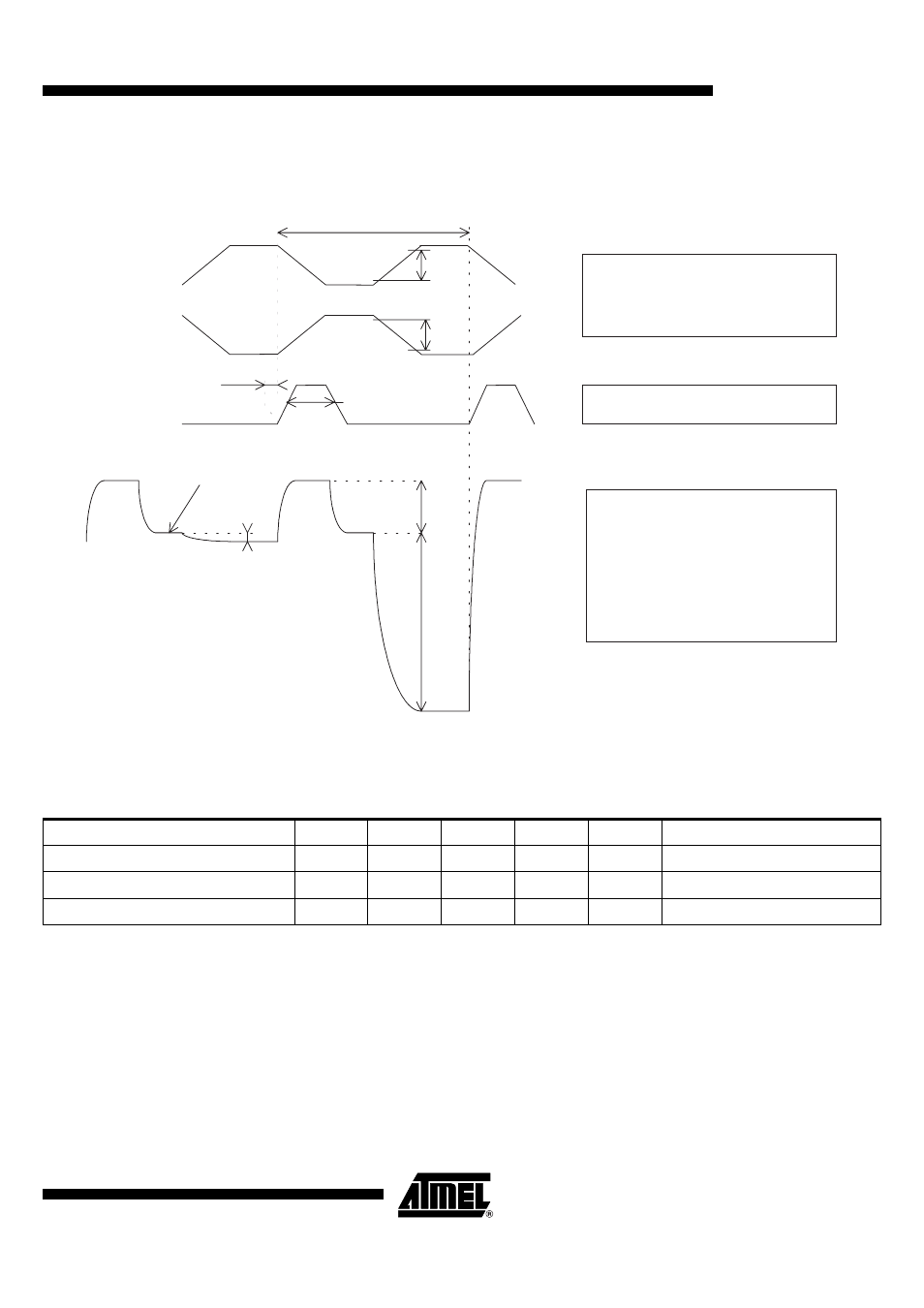
The following diagram shows the detailed timing for the pixel readout:
Figure 3. Pixel Readout Timing Diagram
Exposure Time
Reduction
The TH7815ACC antiblooming structure provides an electronic shutter capability by
clocking phase
Φ
A during the line period. The timing diagram is described below:
L1
Φ
L2
Φ
R
Φ
10%
90%
90%
10%
tr
tf
Tpixel
≥
0 ns
≥
10 ns
50%
Video signal
Reset Feedthrough
Offset in darkness
VIDEO OUTPUTS
±
floating diode level
Duty cycle: 50%
±
10%
Crossover at 50%
±
10%
Rise and fall time
≤
10 ns
Rise and fall time
≤
8 ns
Video outputs are synchronous
Video signal occurs on
Φ
L2 falling edge
First useful pixel occurs on 5th
falling edge of
Φ
L2 after
Φ
P
Antiblooming Gate
Φ
A
Min.
Typ.
Max.
Unit
Clock Capacitance < 200 pF
High Level
8.5
9
9.5
V
Low Level Sets Saturation Level
Low Level
2
4
7
V
See Pixel Saturation Adjustment
Pulse Min.
200 ns