Rainbow Electronics MAX5098A User Manual
Page 23
MAX5098A
Dual, 2.2MHz, Automotive Buck or Boost
Converter with 80V Load-Dump Protection
______________________________________________________________________________________
23
3) Place a zero
where
and R
F
≥ 10kΩ.
4) Calculate C
I
for a target unity crossover frequency, f
C
.
5) Place a pole
or 5 x f
C
, whichever
is lower,
6) Place a second zero, f
Z2
, at 0.2 x f
C
or at f
LC
,
whichever is lower.
7) Place a second pole at 1/2 the switching frequency.
Boost Converter Compensation
The boost converter compensation gets complicated
due to the presence of a right-half-plane zero
f
ZERO,RHP
. The right-half-plane zero causes a drop in
phase while adding positive (+1) slope to the gain
curve. It is important to drop the gain significantly below
unity before the RHP frequency. Use the following pro-
cedure to calculate the compensation components:
1) Calculate the LC double-pole frequency, f
LC
, and
the right-half-plane-zero frequency.
where
D
V
V
R
V
I
IN
OUT
MIN
OUT
OUT MAX
=
=
−
( )
1
(
)
f
D R
L
ZERO RHP
MIN
OUT
,
=
( )
×
−
( )
1
2
2
π
f
D
L
C
LC
OUT
OUT
=
Ч
Ч
−
1
2
π
C
C
f
R
C
CF
F
SW
F
F
=
Ч
Ч
Ч
Ч
(
)
−
2
0 5
1
π
.
R
f
C
R
Z
I
I
1
1
2
2
=
Ч
Ч
−
π
R
f
C
I
P
I
=
Ч
Ч
1
2
1
π
C
f
L
C
V
V
R
I
C
OUT
OUT
OSC
IN
F
=
Ч Ч
Ч
Ч
Ч
2
π
C
f
R
F
LC
F
=
Ч
Ч
Ч
1
2
0 75
π
.
f
R
C
at
f
Z
F
F
LC
1
1
2
0 75
=
Ч
Ч
Ч
π
.
.
R1
R
F
COMP_
V
OUT
V
REF
R2
R
I
C
I
C
F
C
CF
-
+
g
M
FB_
Figure 5. Type III Compensation Network
PGND_
DRAIN_
MAX5098A
V
L
VDRV
V+
V
OUT_
BST_/VDD_
C
OUT
SGND
PGND_
DRAIN_
SOURCE_
SOURCE_
FB_
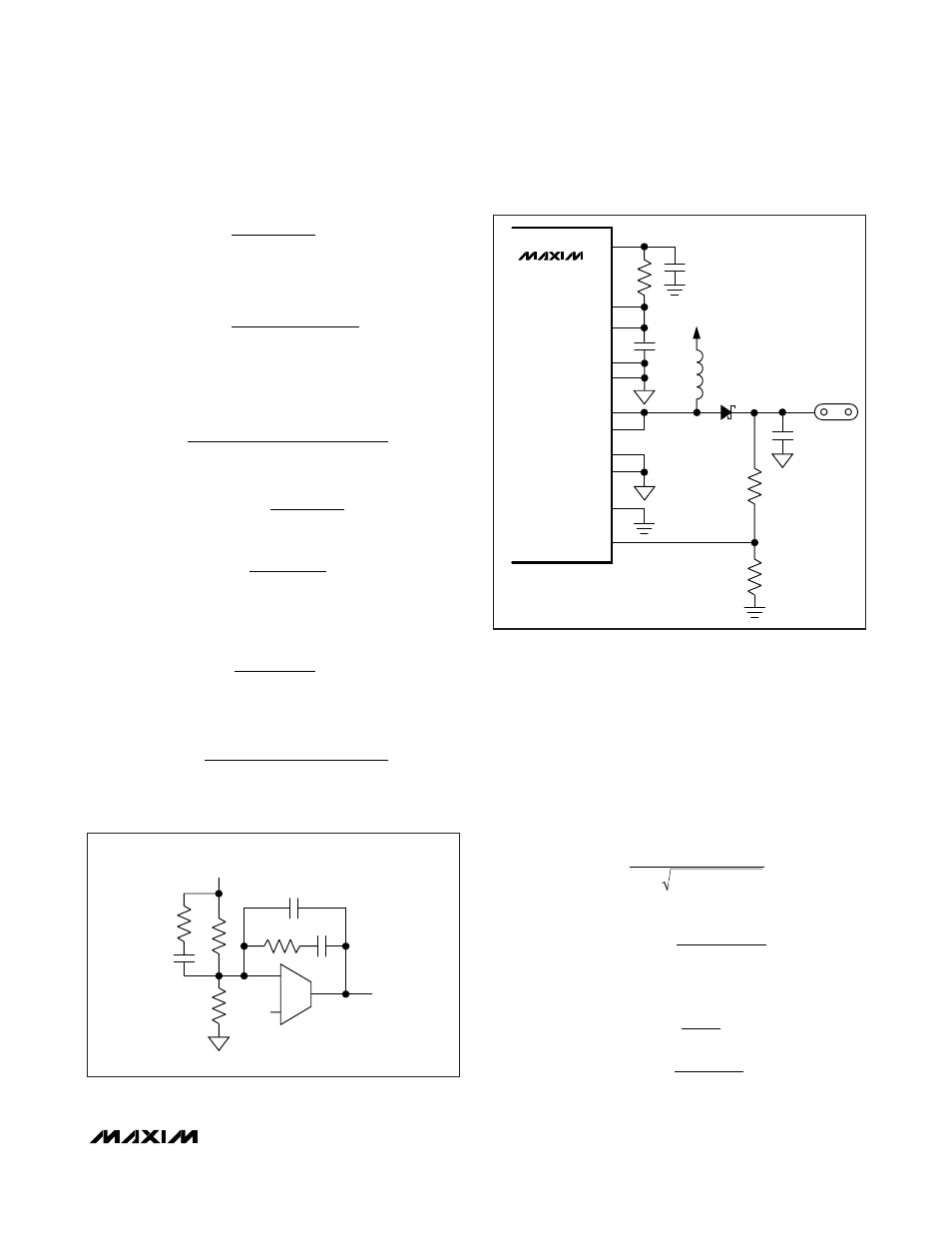
Figure 6. Boost Application
f
R
C
at f
P
I
I
ZERO ESR
1
1
2
=
Ч Ч
π
,