Applications information – Rainbow Electronics MAX5098A User Manual
Page 18
MAX5098A
Dual, 2.2MHz, Automotive Buck or Boost
Converter with 80V Load-Dump Protection
18
______________________________________________________________________________________
Applications Information
Setting the Switching Frequency
The controller generates the clock signal by dividing
down the internal oscillator f
OSC
or the SYNC input sig-
nal when driven by an external oscillator. The switching
frequency equals half the internal oscillator frequency
(f
SW
= f
OSC
/2). The internal oscillator frequency is set
by a resistor (R
OSC
) connected from OSC to SGND. To
find R
OSC
for each converter switching frequency f
SW
,
use the formulas:
A rising clock edge on SYNC is interpreted as a syn-
chronization input. If the SYNC signal is lost, the inter-
nal oscillator takes control of the switching rate,
returning the switching frequency to that set by R
OSC
.
When an external synchronization signal is used, R
OSC
must be selected such that f
SW
= 1/2 f
SYNC
. When
f
SYNC
clock signal is applied, f
CKO
equals f
SYNC
wave-
form, phase shifted by 180°. If the MAX5098A is run-
ning without external synchronization, f
CKO
equals the
internal oscillator frequency f
OSC
.
Buck Converter
Effective Input Voltage Range
Although the MAX5098A converter can operate from
input supplies ranging from 5.2V to 19V, the input volt-
age range can be effectively limited by the MAX5098A
duty-cycle limitations for a given output voltage. The
maximum input voltage is limited by the minimum on-
time (t
ON(MIN)
):
where t
ON(MIN)
is 100ns. The minimum input voltage is
limited by the maximum duty cycle (D
MAX
= 0.82):
where V
DROP1
is the total parasitic voltage drops in the
inductor discharge path, which includes the forward
voltage drop (V
D
) of the rectifier, the series resistance
of the inductor, and the PCB resistance. V
DROP2
is the
total resistance in the charging path that includes the
on-resistance of the high-side switch, the series resis-
tance of the inductor, and the PCB resistance.
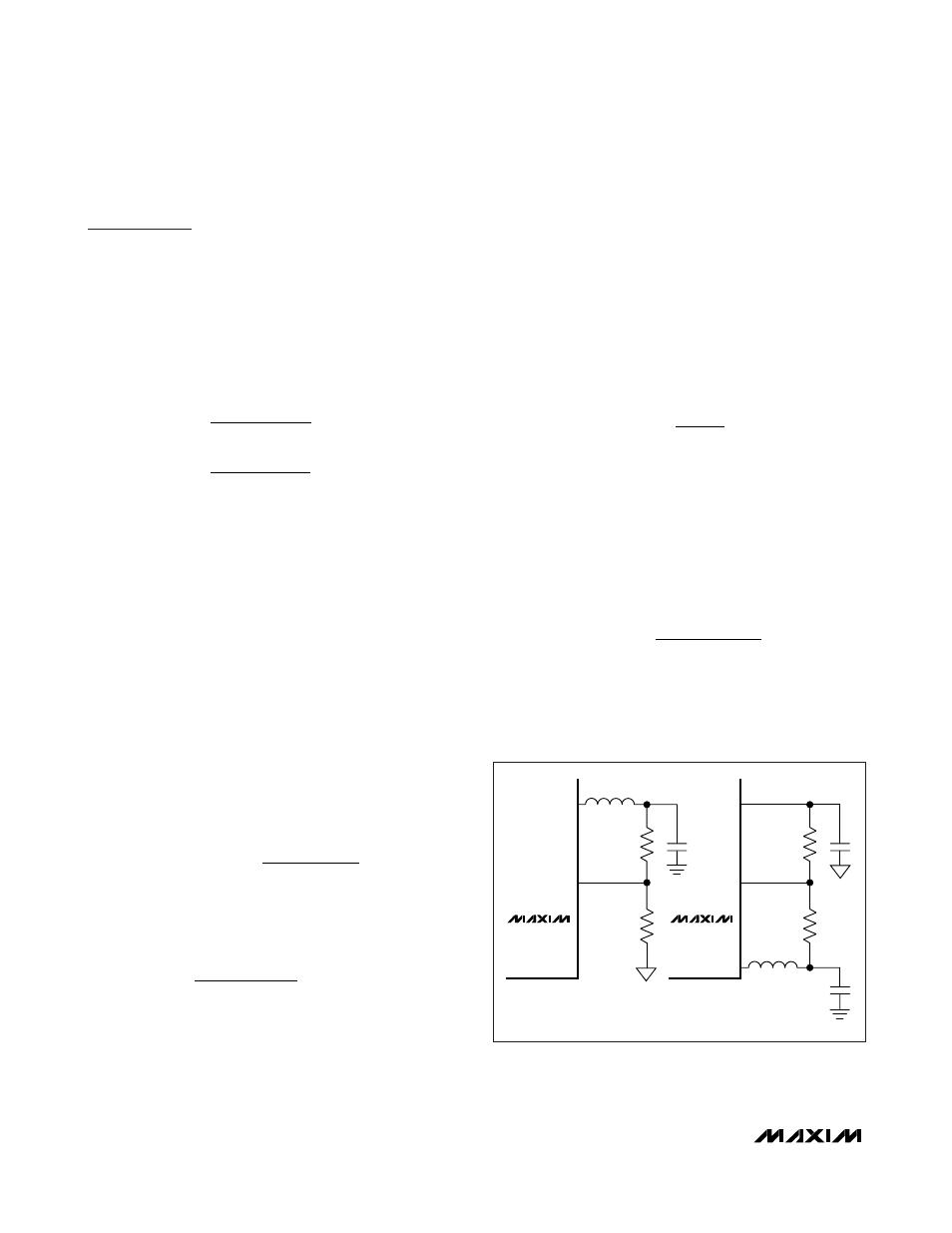
Setting the Output Voltage
For 0.8V or greater output voltages, connect a voltage-
divider from OUT_ to FB_ to SGND (Figure 3). Select R
B
(FB_ to SGND resistor) to between 1kΩ and 20kΩ.
Calculate R
A
(OUT_ to FB_ resistor) with the following
equation:
where V
FB_
= 0.8V (see the
Electrical Characteristics
table) and V
OUT_
can range from V
FB_
to 28V (boost
operation).
For output voltages below 0.8V, set the MAX5098A out-
put voltage by connecting a voltage-divider from OUT_
to FB_ to BYPASS (Figure 3). Select R
C
(FB_ to BYPASS
resistor) in the 50kΩ range. Calculate R
A
with the fol-
lowing equation:
where V
FB_
= 0.8V, V
BYPASS
= 2V (see the
Electrical
Characteristics
table), and V
OUT_
can range from 0V to
V
FB_
.
R
R
V
V
V
V
A
C
FB
OUT
BYPASS
FB
=
⎡
⎣
⎢
⎢
⎤
⎦
⎥
⎥
−
−
_
_
_
R
R
V
V
A
B
OUT
FB
=
⎛
⎝
⎜
⎞
⎠
⎟
⎡
⎣
⎢
⎢
⎤
⎦
⎥
⎥
−
_
_
1
V
V
V
D
V
V
IN MIN
OUT
DROP
MAX
DROP
DROP
(
)
=
+
⎡
⎣
⎢
⎤
⎦
⎥ +
−
1
2
1
V
V
t
f
IN MAX
OUT
ON MIN
SW
(
)
(
)
≤
×
R
k
f
MHz
f
MHz
R
k
f
MHz
f
MHz
OSC
SW
SW
OSC
SW
SW
Ω
Ω
( )
=
(
)
≥
(
)
( )
=
(
)
<
(
)
10 721
1 25
12 184
1 25
0 920
0 973
.
.
.
.
.
.
R
A
V
OUT_
V
OUT_
SOURCE_
FB_
V
OUT_
≥ 0.8V
R
B
MAX5098A
R
C
FB_
SOURCE_
BYPASS
V
OUT_
< 0.8V
R
A
MAX5098A
Figure 3. Adjustable Output Voltage