Rainbow Electronics MAX5098A User Manual
Page 22
MAX5098A
Dual, 2.2MHz, Automotive Buck or Boost
Converter with 80V Load-Dump Protection
22
______________________________________________________________________________________
bandwidth and phase margin. Use a simple pole-zero
pair (Type II) compensation if the output capacitor ESR
zero frequency is below the unity-gain crossover fre-
quency (f
C
). Type III compensation is necessary when
the ESR zero frequency is higher than f
C
or when com-
pensating for a continuous mode boost converter that
has a right-half-plane zero.
Use procedure 1 to calculate the compensation net-
work components when f
ZERO,ESR
< f
C
.
Buck Converter Compensation
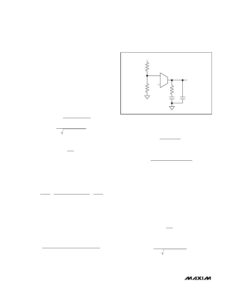
Procedure 1 (See Figure 4)
1) Calculate the f
ZERO,ESR
and LC double-pole fre-
quencies:
2) Select the unity-gain crossover frequency:
If the f
ZERO,ESR
is lower than f
C
and close to f
LC
, use a
Type II compensation network where R
F
C
F
provides a
midband zero f
MID,ZERO
, and R
F
C
CF
provides a high-
frequency pole.
3) Calculate modulator gain G
M
at the crossover fre-
quency.
where V
OSC
is a peak-to-peak ramp amplitude equal to
1V.
The transconductance error amplifier gain is:
G
E/A
= g
M
x R
F
The total loop gain at f
C
should be equal to 1:
G
M
x G
E/A
= 1
or
4) Place a zero at or below the LC double pole:
5) Place a high-frequency pole at f
P
= 0.5 x f
SW
.
Procedure 2 (See Figure 5)
If the output capacitor used is a low-ESR ceramic type,
the ESR frequency is usually far away from the targeted
unity crossover frequency (f
C
). In this case, Type III
compensation is recommended. Type III compensation
provides two-pole zero pairs. The locations of the zero
and poles should be such that the phase margin peaks
around f
C
. It is also important to place the two zeros at
or below the double pole to avoid the conditional stabil-
ity issue.
1) Select a crossover frequency:
2) Calculate the LC double-pole frequency, f
LC
:
f
L
C
LC
OUT
OUT
=
Ч
Ч
1
2
π
f
f
C
SW
≤
20
C
C
f
R
C
CF
F
SW
F
F
=
Ч
Ч
Ч
(
)
−
2
0 5
1
π
.
C
R
f
F
F
LC
=
Ч
Ч
1
2
π
R
V
ESR
f
L
V
V
g
ESR
F
OSC
C
OUT
OUT
IN
M
=
+
Ч Ч
(
)
Ч
Ч
Ч
Ч
2
0 8
π
.
G
V
V
ESR
ESR
f
L
V
M
IN
OSC
C
OUT
OUT
=
Ч
+
Ч Ч
(
)
Ч
2
0 8
π
.
f
f
C
SW
≤
20
f
ESR C
f
L
C
ZERO ESR
OUT
LC
OUT
OUT
,
=
Ч
Ч
=
Ч
1
2
1
2
π
π
R
1
FB_
R
F
COMP_
V
OUT
V
REF
C
CF
C
F
R
2
-
+
g
M
Figure 4. Type II Compensation Network