Pgood, Current limit, Output overvoltage protection – Rainbow Electronics MAX5098A User Manual
Page 17: Thermal-overload protection
MAX5098A
Dual, 2.2MHz, Automotive Buck or Boost
Converter with 80V Load-Dump Protection
______________________________________________________________________________________
17
PGOOD_
Converter 1 and converter 2 include a power-good flag,
PGOOD1 and PGOOD2, respectively. Since PGOOD_
is an open-drain output and can sink 3mA while provid-
ing the TTL logic-low signal, pull PGOOD_ to a logic
voltage to provide a logic-level output. PGOOD1 goes
low when converter 1’s feedback FB1 drops to 92.5%
(V
TPGOOD_
) of its nominal set point. The same is true for
converter 2. Connect PGOOD_ to SGND or leave
unconnected if not used.
Current Limit
The internal MOSFET switch current of each converter is
monitored during its on-time. When the peak switch cur-
rent crosses the current-limit threshold of 3.45A (typ) and
2.1A (typ) for converter 1 and converter 2, respectively,
the on-cycle is terminated immediately and the inductor
is allowed to discharge. The MOSFET is turned on at the
next clock pulse, initiating a new switching cycle.
In deep overload or short-circuit conditions when the
V
FB_
voltage drops below 0.2V, the switching frequen-
cy is reduced to 1/4 x f
SW
to provide sufficient time for
the inductor to discharge. During overload conditions, if
the voltage across the inductor is not high enough to
allow for the inductor current to properly discharge,
current runaway may occur. Current runaway can
destroy the device in spite of internal thermal-overload
protection. Reducing the switching frequency during
overload conditions allows more time for inductor dis-
charge and prevents current runaway.
Output Overvoltage Protection
The MAX5098A outputs are protected from output volt-
age overshoots due to input transients and shorting the
output to a high voltage. When the output voltage rises
above the overvoltage threshold, 110% (typ) nominal
FB_, the overvoltage condition is triggered. When the
overvoltage condition is triggered on either channel,
both converters are immediately turned off, 20Ω pull-
down switches from SOURCE_ to PGND_ are turned on
to help the output-voltage discharge, and the gate of
the load-dump protection external MOSFET is pulled
low. The device restarts as soon as both converter out-
puts discharge, bringing both FB_ input voltages below
12.5V of their nominal set points.
Thermal-Overload Protection
During continuous short circuit or overload at the out-
put, the power dissipation in the IC can exceed its limit.
The MAX5098A provides thermal shutdown protection
with temperature hysteresis. Internal thermal shutdown
is provided to avoid irreversible damage to the device.
When the die temperature exceeds +165°C (typ), an
on-chip thermal sensor shuts down the device, forcing
the internal switches to turn off, allowing the IC to cool.
The thermal sensor turns the part on again with soft-
start after the junction temperature cools by +20°C.
During thermal shutdown, both regulators shut down,
PGOOD_ goes low, and soft-start resets. The internal
20V zener clamp from IN_HIGH to SGND is not turned
off during thermal shutdown because clamping action
must be always active.
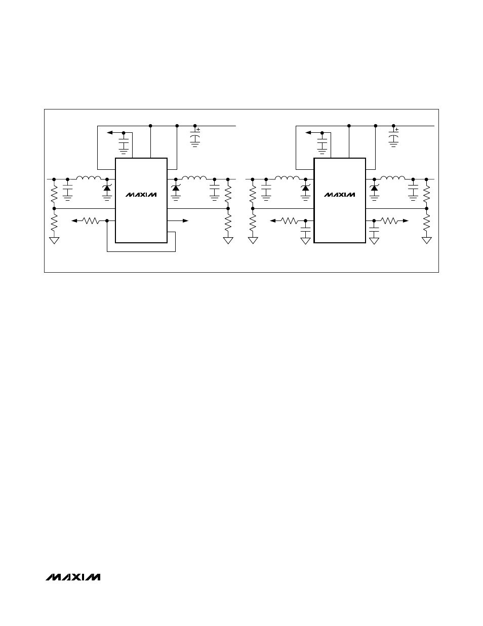
FB1
FB2
EN1
EN2
V
L
R1
R2
C1
C2
V
L
V
L
V+
MAX5098A
OUTPUT2
OUTPUT1
DRAIN2
SOURCE2
DRAIN1
SOURCE1
V
IN
V
L
FB1
FB2
EN1
EN2
SEQUENCING—OUTPUT 2 DELAYED WITH RESPECT TO OUTPUT 1.
R1/C1 AND R2/C2 ARE SIZED FOR REQUIRED SEQUENCING.
V
L
V
L
V
L
V+
MAX5098A
OUTPUT2
OUTPUT1
DRAIN2
SOURCE2
DRAIN1
SOURCE1
PGOOD1
V
IN
V
L
Figure 2. Power-Supply Sequencing Configurations