Typical operating characteristics (continued), Pin description – Rainbow Electronics MAX7473 User Manual
Page 6
MAX7472/MAX7473
HDTV Anti-Aliasing Filters with Triple-Input Mux
6
_______________________________________________________________________________________
-40
-10
-15
-20
-25
-30
-35
0
-5
5
10
0.1
10
1
100
1000
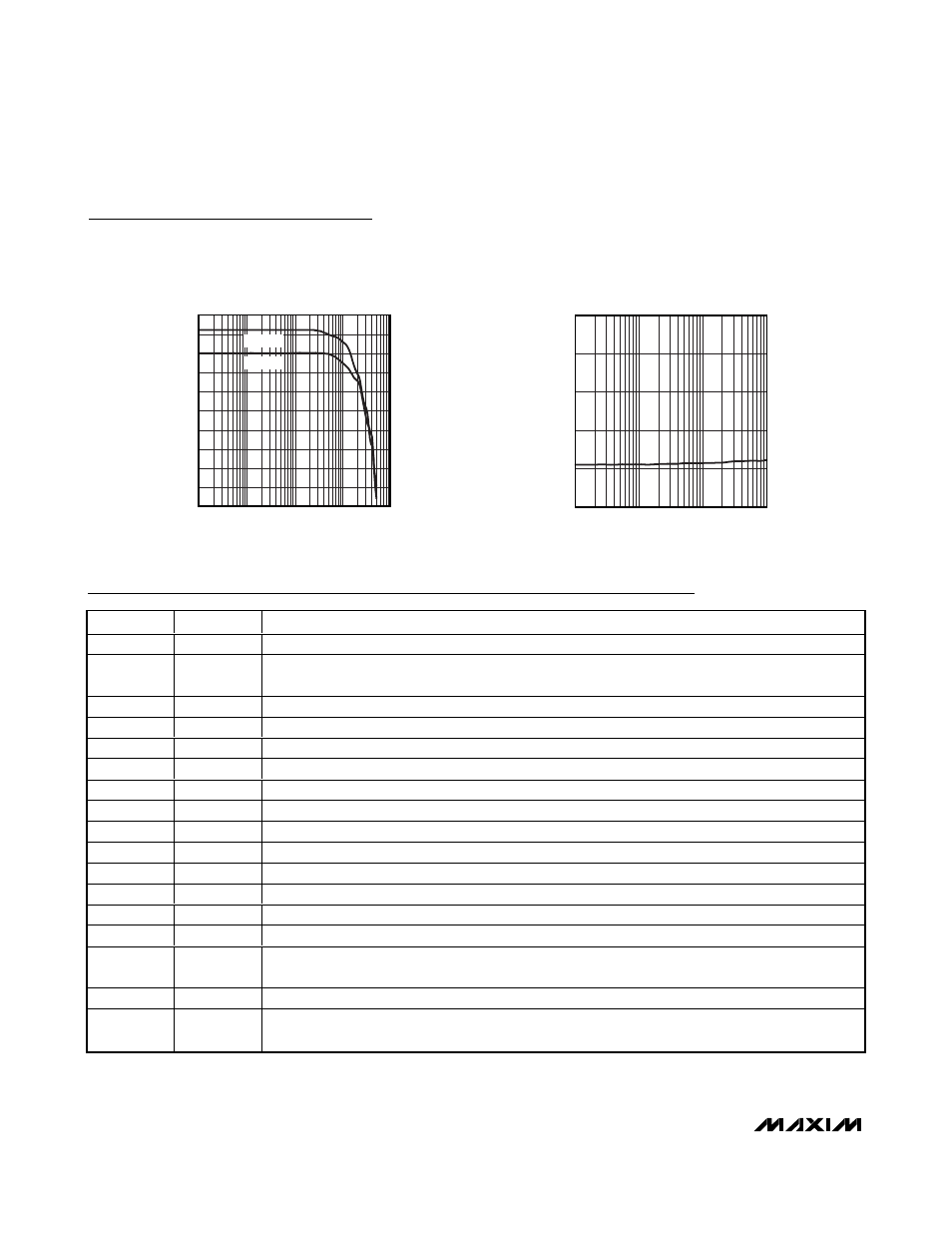
BYPASS-MODE FREQUENCY RESPONSE
MAX7472/73 toc10
FREQUENCY (MHz)
RESPONSE (dB)
MAX7473
MAX7472
0
4
12
8
16
20
0.1
10
1
100
BYPASS-MODE GROUP DELAY
MAX7472/73 toc11
FREQUENCY (MHz)
DELAY (ns)
Typical Operating Characteristics (continued)
(AV
DD
= +5V, DV
DD
= 3.3V, R
LOAD
= 150Ω to GND, C
IN
= 0.1µF, T
A
= +25°C.)
Pin Description
PIN
NAME
FUNCTION
1
INC1
Channel C Input 1. AC-couple INC1 with a series 0.1µF capacitor.
2, 6, 25, 26
AGND
Analog Ground. Connect all AGND pins to the ground plane. See the Power-Supply Bypassing and
Layout Considerations section.
3
INA2
Channel A Input 2. AC-couple INA2 with a series 0.1µF capacitor.
4
INB2
Channel B Input 2. AC-couple INB2 with a series 0.1µF capacitor.
5
INC2
Channel C Input 2. AC-couple INC2 with a series 0.1µF capacitor.
7
INA3
Channel A Input 3. AC-couple INA3 with a series 0.1µF capacitor.
8
INB3
Channel B Input 3. AC-couple INB3 with a series 0.1µF capacitor.
9
INC3
Channel C Input 3. AC-couple INC3 with a series 0.1µF capacitor.
10
DGND
Digital Ground. See the Power-Supply Bypassing and Layout Considerations section.
11
SYNCA
Channel A External Sync Input. Connect to ground if not used.
12
SYNCB
Channel B External Sync Input. Connect to ground if not used.
13
SYNCC
Channel C External Sync Input. Connect to ground if not used.
14
SCL
I
2
C-Compatible Serial Clock Input
15
SDA
I
2
C-Compatible Serial Data Input/Output
16
DV
DD
Digital Power Supply. Bypass to DGND with a 0.1µF capacitor. See the Power-Supply Bypassing and
Layout Considerations section.
17
OUT3
Video Output 3. OUT3 can be either AC- or DC-coupled.
18, 20, 22
AV
DD
Analog Power Supply. Bypass each AV
DD
input to AGND using a 0.1µF capacitor. See the Power-
Supply Bypassing and Layout Considerations section.