Rainbow Electronics MAX7473 User Manual
Page 11
tion). After receiving the proper address, the
MAX7472/MAX7473 (slave) issue an ACK by pulling
SDA low for one clock cycle.
The MAX7472/MAX7473 slave address consists of 5
fixed bits A6–A2 (set to 10010) followed by 2 pin-pro-
grammable bits A1 and A0. The most significant address
bit (A6) is transmitted first, followed by the remaining
bits. Addresses A1 and A0 can also be driven dynami-
cally if required, but the values must be stable when they
are expected in the address sequence.
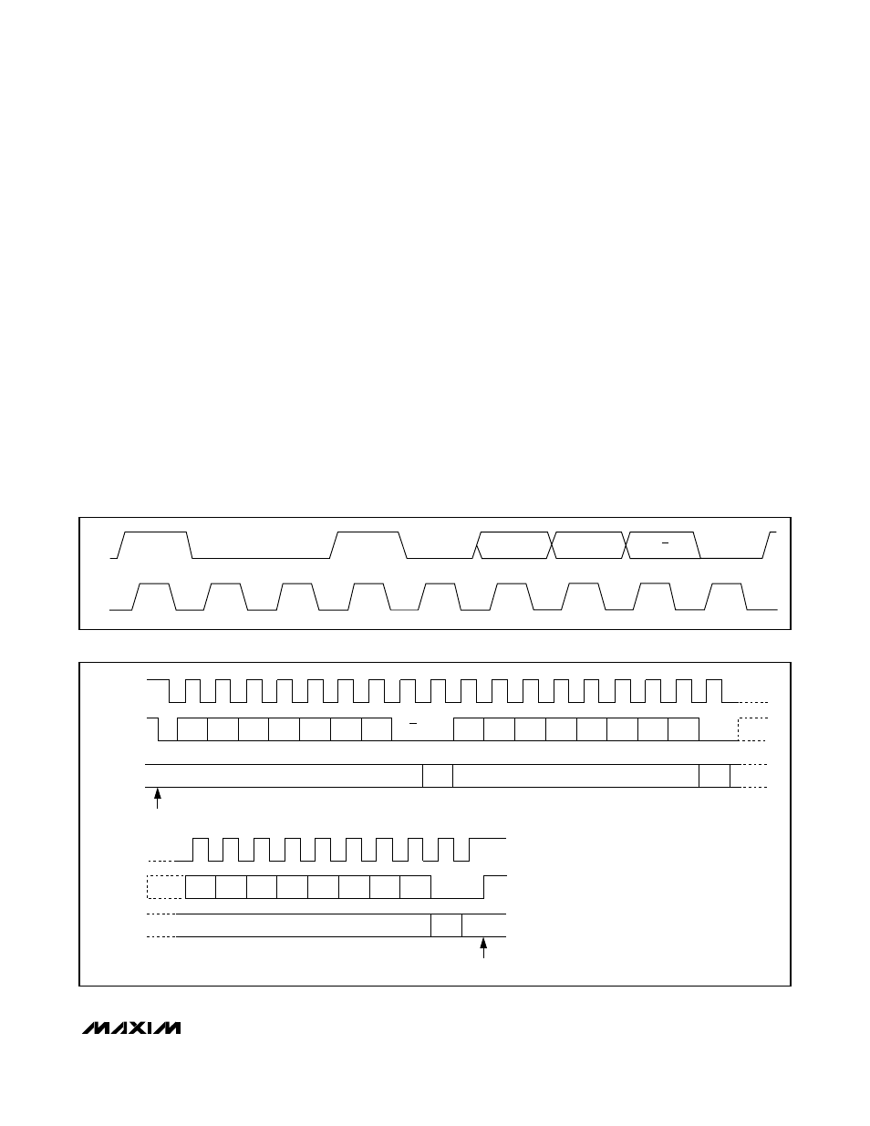
Command Byte (Write Cycle)
A write cycle begins with the bus master issuing a
START condition followed by 7 address bits (Figure 5)
and a write bit (R/W = 0). After successfully receiving
its address, the MAX7472/MAX7473 (slave) issue an
ACK. The MAX7472/MAX7473 recognize the next byte
after a successfully received address as the command
byte (Table 3).
Use the command byte to configure the MAX7472/
MAX7473. While most of the commands listed in Table
3 modify the functionality of the MAX7472/
MAX7473, some commands prepare the device for fur-
ther data transfers (see the
Control/Status Register
,
Frequency Register
, and
Channel-Selection Register
sections.) When the write cycle is prematurely aborted,
the register is not updated. Figures 6 and 7 show
examples of write sequences.
MAX7472/MAX7473
HDTV Anti-Aliasing Filters with Triple-Input Mux
______________________________________________________________________________________
11
SDA
SCL
1
0
1
0
A1
A0
0
R/W
MSB
LSB
ACK
Figure 5. Slave-Address Byte Definition
SDA
SCL
1
0
0
1
0
A1
A0
R/W
C7
C6
C5
C4
C3
C2
C1
C0
ACK
ACK
OUT
IN
OUT
IN TO MAX7472/MAX7473
SDA (CONT)
SDA
DIRECTION
SDA
DIRECTION
SCL (CONT)
F7
F6
F5
F4
F3
F2
F1
ACK
OUT
F0
IN
IN
START
STOP
COMMAND WORD C7–C0 IS 00010010.
0
0
0
1
0
0
1
0
Figure 6. Write Sequence to Update the Frequency Register