Timing characteristics – Rainbow Electronics MAX7473 User Manual
Page 4
MAX7472/MAX7473
HDTV Anti-Aliasing Filters with Triple-Input Mux
4
_______________________________________________________________________________________
TIMING CHARACTERISTICS
(AV
DD
= +5V ±5%, DV
DD
= 2.7V to 3.6V, T
A
= 0°C to +85°C, unless otherwise noted. Typical values are at T
A
= +25°C.) (Figure 1)
PARAMETER
SYMBOL
CONDITIONS
MIN
TYP
MAX
UNITS
Serial Clock Frequency
f
SCL
0
400
kHz
Bus Free Time Between STOP (P)
and START (S) Conditions
t
BUF
1.3
µs
Hold Time (Repeated) START (Sr)
Condition
t
HD;STA
After this period, the first clock pulse is
generated
0.6
µs
SCL Pulse-Width Low
t
LOW
1.3
µs
SCL Pulse-Width High
t
HIGH
0.6
µs
Setup Time for a Repeated START
(Sr) Condition
t
SU;STA
0.6
µs
Data Hold Time
t
HD;DAT
(Note 5)
0
0.9
µs
Data Setup Time
t
SU;DAT
100
ns
Rise Time of Both SDA and SCL
Signals, Receiving
t
r
0
300
ns
Fall Time of Both SDA and SCL
Signals, Receiving
t
f
0
300
ns
Fall Time of SDA Signal,
Transmitting
t
f
(Note 6)
20 +
0.1C
b
300
ns
Setup Time for STOP (P) Condition
t
SU;STO
0.6
µs
Capacitive Load for Each Bus Line
C
b
400
pF
Pulse Width of Spikes Suppressed
by the Input Filter
t
SP
(Note 7)
0
50
ns
Note 1: The filter passband edge is set to code 255.
Note 2: The filter passband edge is set to code 40.
Note 3: 1H is the total line period, depending on the video standard. For NTSC, this is 63.5µs, for HDTV, the line period is 29.64µs.
Note 4: The clamp level is at the sync tip for signals with sync pulses, and is at the blanking level otherwise.
Note 5: A master device must provide a hold time of at least 300ns for the SDA signal (referred to V
IL
of the SCL signal) to bridge
the undefined region of SCL’s falling edge.
Note 6: C
b
= total capacitance of one bus line in pF. t
R
and t
F
measured between 0.3V
DD
and 0.7V
DD
.
Note 7: Input filters on the SDA and SCL inputs suppress noise spikes less than 50ns.
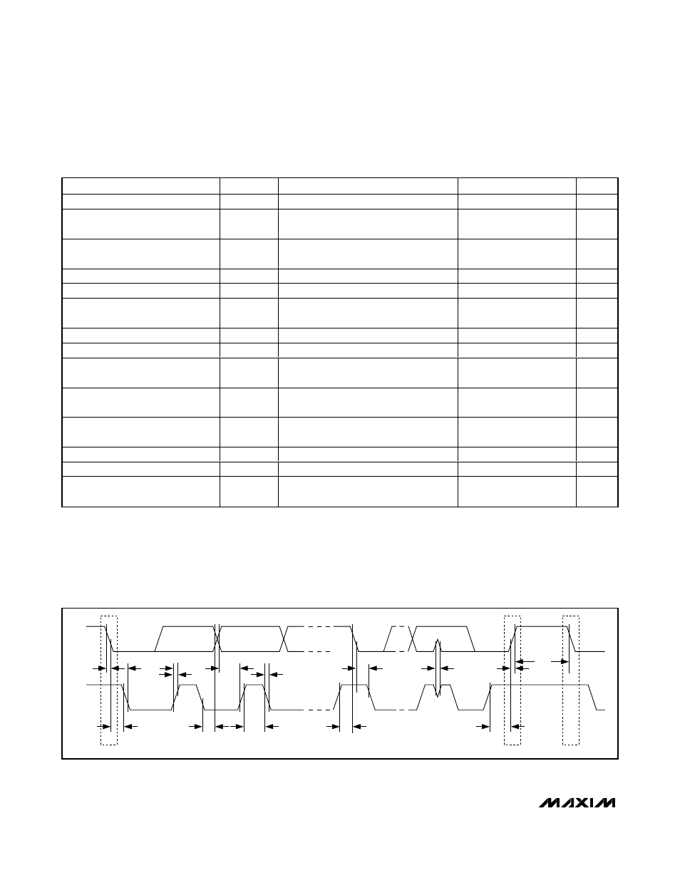
SDA
SCL
t
r
t
f
S
r
t
SP
t
r
P
S
t
LOW
t
HD;STA
t
HD;DAT
t
SU;STA
t
HIGH
t
SU;DAT
t
HD;STA
t
SU;STO
t
BUF
t
f
S
Figure 1. 2-Wire Serial-Interface Timing Diagram