Rainbow Electronics MAX7473 User Manual
Page 2
MAX7472/MAX7473
HDTV Anti-Aliasing Filters with Triple-Input Mux
2
_______________________________________________________________________________________
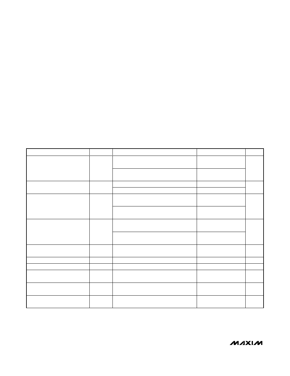
ABSOLUTE MAXIMUM RATINGS
ELECTRICAL CHARACTERISTICS
(AV
DD
= +5V ±5%, DV
DD
= 2.7V to 3.6V, R
LOAD
= 150Ω to AGND, C
IN
= 0.1µF, T
A
= 0°C to +85°C, unless otherwise noted. Typical
values are at T
A
= +25°C.)
Stresses beyond those listed under “Absolute Maximum Ratings” may cause permanent damage to the device. These are stress ratings only, and functional
operation of the device at these or any other conditions beyond those indicated in the operational sections of the specifications is not implied. Exposure to
absolute maximum rating conditions for extended periods may affect device reliability.
AV
DD
to AGND .........................................................-0.3V to +6V
DV
DD
to DGND.........................................................-0.3V to +4V
AGND to DGND.....................................................-0.3V to +0.3V
INA_, INB_, INC_ to AGND...........................................................
............................-0.3V to the lower of (AV
DD
+ 0.3V) and +6V
OUT_ to AGND.…..-0.3V to the lower of (AV
DD
+ 0.3V) and +6V
SYNC_, A_ to AGND.....................................................................
...............................-0.3V to the lower of (AV
DD
+ 0.3V) and +6V
SCL, SDA to DGND .................................................-0.3V to + 6V
Maximum Current into Any Pin
(except AV
DD
, DV
DD
, and OUT) ...................................±50mA
Continuous Power Dissipation (T
A
= +70°C)
28-Pin TQFN (derate 34.5mW/°C above +70°C) ........2758mW
Operating Temperature Range.............................. 0°C to +85°C
Storage Temperature Range ............................-65°C to +150°C
Junction Temperature ......................................................+150°C
Lead Temperature (soldering, 10s) .................................+300°C
PARAMETER
SYMBOL
CONDITIONS
MIN
TYP
MAX
UNITS
HD: f = 100kHz to 30MHz, relative to 100kHz
(Note 1)
-3
-0.6
+1
Filter Passband Response
A
PB
SD: f = 100kHz to 5.75MHz, relative to
100kHz (Note 2)
±0.1
±1.0
dB
HD: f = 74MHz (Note 1)
57
Filter Stopband Attenuation
A
SB
SD: f = 27MHz (Note 2)
63
dB
HD: 100kHz to 30MHz, relative to 100kHz
(Note 1)
20
Group-Delay Deviation
Δt
G
SD: 100kHz to 5.75MHz, relative to 100kHz
(Note 2)
15
ns
HD: channel to channel, 100kHz to 2MHz
(Note 1)
5
Group-Delay Matching
t
G(MATCH)
SD: channel to channel, 100kHz to 500kHz
(Note 2)
1.5
ns
Bypass Frequency Response
-3dB, bypass mode, independent of filter
setting
100
MHz
SD Differential Gain
dG
5-step modulated staircase (Note 2)
0.25
%
SD Differential Phase
d
φ
5-step modulated staircase (Note 2)
0.25
D egr ees
Signal-to-Noise Ratio
SNR
Output signal (2V
P-P
) to RMS noise (100kHz
to 30MHz) (Note 1)
69
dB
SD Line-Time Distortion
H
DIST
Deviations in a line with an 18µs, 100 IRE bar,
1 line = 63.5µs (Note 2)
0.3
%
SD Field-Time Distortion
V
DIST
Deviations in 130 lines with 18µs, 100 IRE
bars (Note 2)
0.3
%