Max5099 – Rainbow Electronics MAX5099 User Manual
Page 23
MAX5099
2) Place a zero
where R
F
≥ 10kΩ.
3) Calculate C
I
for a target crossover frequency, f
C
:
where
ω
C
= 2
π x f
C
.
4) Place a pole
or 5 x f
C
, whichever is lower.
5) Place the second zero
6) Place the second pole at 1/2 the switching frequency.
Load-Dump Protection MOSFET
Select the external MOSFET with an adequate voltage
rating, V
DSS
, to withstand the maximum expected load-
dump input voltage. The on-resistance of the MOSFET,
R
DS(ON)
, should be low enough to maintain a minimal
voltage drop at full load, limiting the power dissipation
of the MOSFET.
During regular operation, the power dissipated by the
MOSFET is:
P
NORMAL
= I
LOAD
2
x R
DS(ON)
where I
LOAD
is equal to the sum of both converters’
input currents.
The MOSFET operates in a saturation region during
load dump, with both high voltage and current applied.
Choose a suitable power MOSFET that can safely oper-
ate in the saturation region. Verify its capability to sup-
port the downstream DC-DC converters’ input current
during the load-dump event by checking its safe oper-
ating area (SOA) characteristics.
Since the transient peak power dissipation on the
MOSFET can be very high during the load-dump event,
also refer to the thermal impedance graph given in the
data sheet of the power MOSFET to make sure its tran-
sient power dissipation is kept within the recommended
limits.
Improving Noise Immunity
In applications where the MAX5099 is subject to noisy
environments, adjust the controller’s compensation to
improve the system’s noise immunity. In particular, high-
frequency noise coupled into the feedback loop causes
jittery duty cycles. One solution is to lower the crossover
frequency (see the
Compensation
section).
C
C
f
R
C
CF
F
SW
F
F
=
Ч
Ч
Ч
Ч
(
)
−
2
0 5
1
π
.
R
f
C
R
LC
I
I
1
1
2
=
Ч
Ч
−
π
f
R
C
at f
Z
I
LC
2
1
2
1
=
Ч Ч
π
.
R
f C
I
I
=
Ч Ч
1
2
π
C
V
D
L C
R V
I
OSC
C
O O
C F IN
=
( )
+
⎡
⎣⎢
⎤
⎦⎥
−
1
2
2
ω
ω
C
f
R
F
LC
F
=
Ч
Ч
Ч
1
2
0 75
π
.
f
R
C
at
f
Z
F
F
LC
1
1
2
0 75
=
Ч
Ч
Ч
π
.
.
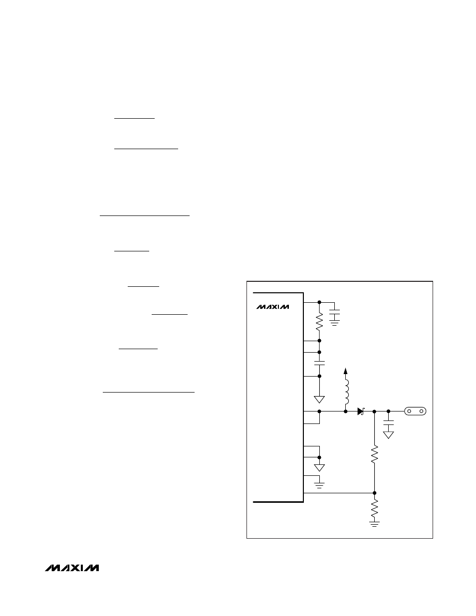
PGND
DRAIN_
MAX5099
V
L
VDRV
V+
VOUT_
BST_/VDD_
C
OUT
SGND
DRAIN_
*DL_
*LEAVE DL_ UNCONNECTED.
SOURCE_
SOURCE_
FB_
Figure 5. Boost Application
Dual, 2.2MHz, Automotive Synchronous Buck
Converter with 80V Load-Dump Protection
______________________________________________________________________________________
23
f
R
C
at f
P
I
I
ZERO RHP
1
1
2
=
Ч Ч
π
,