Rainbow Electronics MAX5099 User Manual
Page 22
MAX5099
Dual, 2.2MHz, Automotive Synchronous Buck
Converter with 80V Load-Dump Protection
22
______________________________________________________________________________________
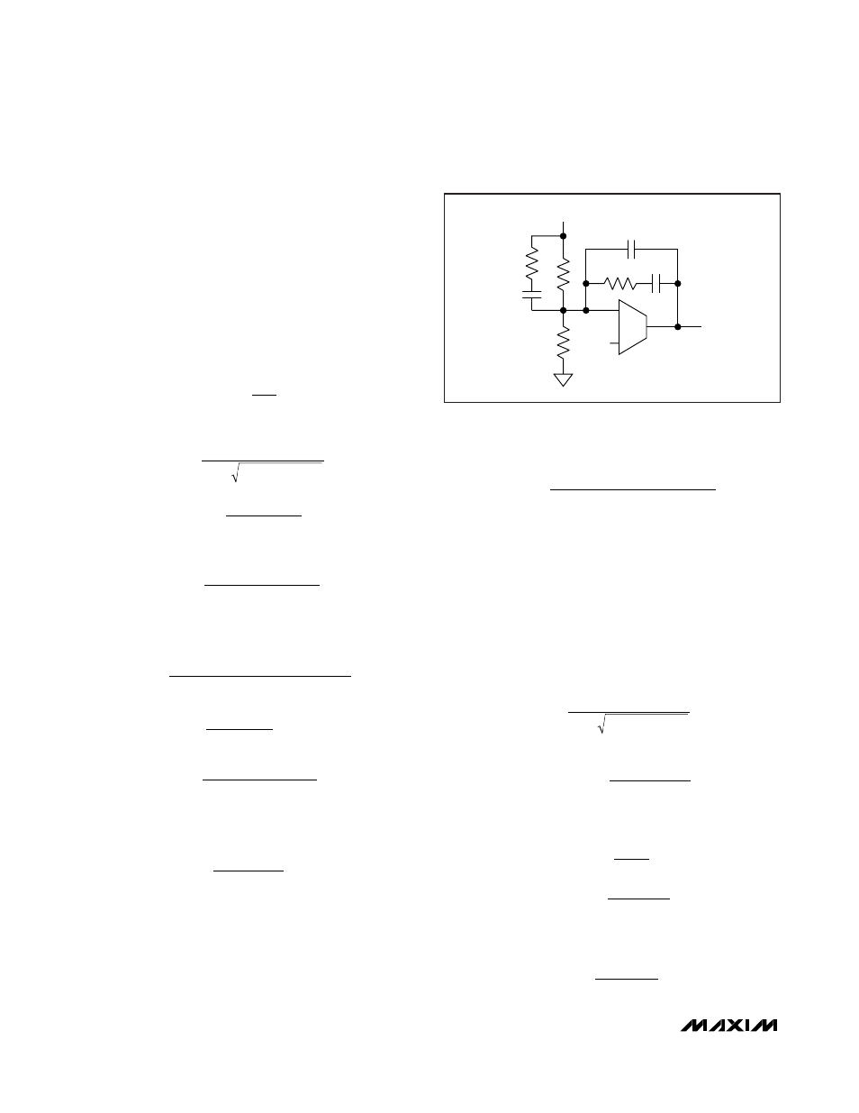
Procedure 2 (See Figure 4)
If the output capacitor used is a low-ESR ceramic type,
the ESR frequency is usually far away from the targeted
unity crossover frequency (f
C
). In this case, Type III
compensation is recommended. Type III compensation
provides two-pole zero pairs. The locations of the zero
and poles should be such that the phase margin peaks
around f
C
. It is also important to place the two zeros at
or below the double pole to avoid the conditional stabil-
ity issue.
1) Select a crossover frequency:
2) Calculate the LC double-pole frequency, f
LC
:
3) Place a zero
where
and R
F
≥ 10kΩ.
4) Calculate C
I
for a target unity crossover frequency, f
C
.
5) Place a pole
6) Place a second zero, f
Z2
, at 0.2 x f
C
or at f
LC
,
whichever is lower.
7) Place a second pole at 1/2 the switching frequency.
Boost Converter Compensation
The boost converter compensation gets complicated
due to the presence of a right-half-plane zero
f
ZERO,RHP
. The right-half-plane zero causes a drop in
phase while adding positive (+1) slope to the gain
curve. It is important to drop the gain significantly below
unity before the RHP frequency. Use the following pro-
cedure to calculate the compensation components:
1) Calculate the LC double-pole frequency, f
LC
, and
the right-half-plane-zero frequency.
where
Target the unity-gain crossover frequency for:
f
f
C
ZERO RHP
≤
,
5
D
V
V
R
V
I
IN
OUT
MIN
OUT
OUT MAX
=
=
−
( )
1
(
)
f
D R
L
ZERO RHP
MIN
OUT
,
=
( )
×
−
( )
1
2
2
π
f
D
L
C
LC
OUT
OUT
=
Ч
Ч
−
1
2
π
C
C
f
R
C
CF
F
SW
F
F
=
Ч
Ч
Ч
Ч
(
)
−
2
0 5
1
π
.
R
f
C
R
Z
I
I
1
1
2
2
=
Ч
Ч
−
π
R
f
C
I
ZERO ESR
I
=
Ч
Ч
1
2
π
,
f
R
C
at f
P
I
I
ZERO ESR
1
1
2
=
Ч Ч
π
.
,
C
f
L
C
V
V
R
I
C
OUT
OUT
OSC
IN
F
=
Ч Ч
Ч
Ч
Ч
2
π
C
f
R
F
LC
F
=
Ч
Ч
Ч
1
2
0 75
π
.
f
R
C
at
f
Z
F
F
LC
1
1
2
0 75
=
Ч
Ч
Ч
π
.
.
f
L
C
LC
OUT
OUT
=
Ч
Ч
1
2
π
f
f
SW
SW
≤
20
R1
R
F
COMP_
V
OUT
V
REF
R2
R
I
C
I
C
F
C
CF
-
+
g
M
FB_
Figure 4. Type III Compensation Network