Pin description – Rainbow Electronics MAX5099 User Manual
Page 11
MAX5099
Dual, 2.2MHz, Automotive Synchronous Buck
Converter with 80V Load-Dump Protection
______________________________________________________________________________________
11
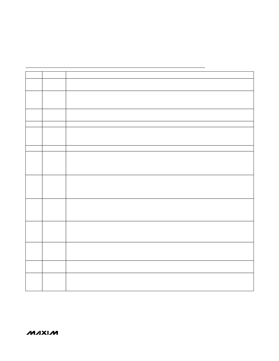
Pin Description
PIN
NAME
FUNCTION
1, 32
SOURCE2
Converter 2 Internal MOSFET Source Connection. For buck converter operation, connect SOURCE2 to the
switched side of the inductor. For boost operation, connect SOURCE2 to PGND (Figure 5).
2, 3
DRAIN2
Converter 2 Internal MOSFET Drain Connection. For buck converter operation, use the MOSFET as a high-
side switch and connect DRAIN2 to the DC-DC converters supply input rail. For boost converter operation,
use the MOSFET as a low-side switch and connect DRAIN2 to the inductor and diode junction (Figure 5).
4
PGOOD2
Converter Open-Drain Power-Good Output. PGOOD2 goes low when converter 2’s output falls below 92.5%
of its set regulation voltage. Use PGOOD2 and EN1 to sequence the converters.
5
EN2
Converter 2 Active-High Enable Input. Connect to V
L
for always-on operation.
6
FB2
Converter 2 Feedback Input. Connect FB2 to a resistive divider between converter 2’s output and SGND to
adjust the output voltage. To set the output voltage below 0.8V, connect FB2 to a resistive voltage-divider
from BYPASS to regulator 2’s output (Figure 2). See the Setting the Output Voltage section.
7
COMP2
Converter 2 Internal Transconductance Amplifier Output. See the Compensation section.
8
OSC
Oscillator Frequency Set Input. Connect a resistor from OSC to SGND (R
OSC
) to set the switching frequency
(see the Setting the Switching Frequency section). Set R
OSC
for an oscillator frequency equal to the SYNC
input frequency when using external synchronization. R
OSC
is still required when an external clock is
connected to the SYNC input. See the Synchronization (SYNC) section.
9
SYNC
External Clock Synchronization Input. Connect SYNC to a 400kHz to 4400kHz clock to synchronize the
switching frequency with the system clock. Each converter frequency is 1/2
of the frequency applied to
SYNC (FSEL_1 = V
L
). For FSEL_1 = SGND, the switching frequency of converter 1 becomes 1/4
of the
SYNC frequency. Connect SYNC to SGND when not used.
10
GATE
Gate Drive Output. Connect to the gate of the external n-channel load-dump protection MOSFET. GATE =
IN_HIGH + 9V (typ) with IN_HIGH = 12V. GATE pulls to IN_HIGH by an internal n-channel MOSFET when V+
raises 2V above IN_HIGH. Leave GATE unconnected if the load-dump protection is not used (MOSFET not
installed).
11
ON/OFF
n-Channel Switch Enable Input. Drive ON/OFF high for normal operation. Drive ON/OFF low to turn off the
external n-channel load-dump protection MOSFET and reduce the supply current to 7μA (typ). When
ON/OFF is driven low, both DC-DC converters are disabled and the PGOOD_ outputs are driven low.
Connect to V+ if the external load-dump protection is not used (MOSFET not installed).
12
IN_HIGH
Startup Input. IN_HIGH is protected by internally clamping to 21V (max). Connect a resistor (4k
Ω max) from
IN_HIGH to the drain of the protection switch. Bypass IN_HIGH with a 4.7μF electrolytic or 1μF minimum
ceramic capacitor. Connect to V+ if the external load-dump protection is not used (MOSFET not installed).
13
V+
Input Supply Voltage. V+ can range from 5.2V to 19V. Connect V+, IN_HIGH, and V
L
together for 4.5V to
5.5V input operation. Bypass V+ to SGND with a 1μF minimum ceramic capacitor.
14
V
L
Internal Regulator Output. The V
L
regulator is used to supply the drive current at input VDRV. When driving
VDRV, use an RC lowpass filter to decouple switching noise from VDRV to the V
L
regulator (see the Typical
Application Circuit). Bypass V
L
to SGND with a 4.7μF minimum ceramic capacitor.