Enable (en1, en2), Pgood, Current limit – Rainbow Electronics MAX5099 User Manual
Page 16: Output overvoltage protection
MAX5099
Dual, 2.2MHz, Automotive Synchronous Buck
Converter with 80V Load-Dump Protection
16
______________________________________________________________________________________
Enable (EN1, EN2)
The MAX5099 dual converter provides separate enable
inputs, EN1 and EN2, to individually control or sequence
the output voltages. These active-high enable inputs are
TTL compatible. Driving EN_ high initiates soft-start of the
converter, and PGOOD_ goes logic-high when the con-
verter output voltage reaches the V
TPGOOD_
threshold.
Driving EN_ low initiates a soft-stop of the converter. Use
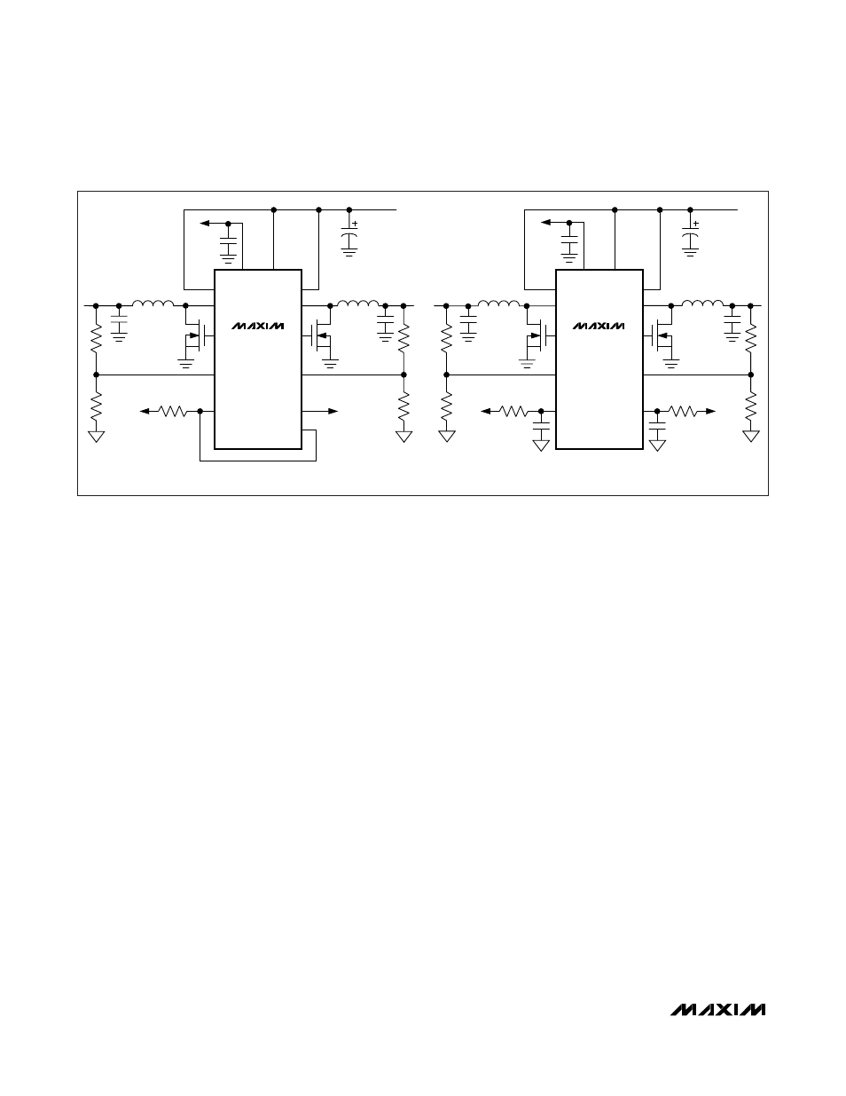
EN1, EN2, and PGOOD1 for sequencing (see Figure 1).
Connect PGOOD1 to EN2 to make sure converter 1’s out-
put is within regulation before converter 2 starts. Add an
RC network from V
L
to EN1 and EN2 to delay the individ-
ual converter. Sequencing reduces input inrush current
and possible chattering. Connect EN_ to V
L
for always-on
operation.
PGOOD_
Converter 1 and converter 2 include power-good flags,
PGOOD1 and PGOOD2, respectively. Since PGOOD_
is an open-drain output and can sink 3mA while provid-
ing the TTL logic-low signal, pull PGOOD_ to a logic
voltage to provide a logic-level output. PGOOD1 goes
low when converter 1’s feedback (FB_) drops to 92.5%
(V
TPGOOD_
) of its nominal set point. The same is true
for converter 2. Connect PGOOD_ to SGND or leave
unconnected, if not used.
Current Limit
The internal high-side MOSFET switch current of each
converter is monitored during its on-time. When the
peak switch current crosses the current-limit threshold
of 3.45A (typ) and 2.1A (typ) for converter 1 and con-
verter 2, respectively, the on-cycle is terminated imme-
diately and the inductor is allowed to discharge. The
MOSFET switch is turned on at the next clock pulse ini-
tiating a new clock cycle.
In deep overload or short-circuit conditions when V
FB
drops below 0.2V, the switching frequency is reduced to
1/4 x f
SW
to provide sufficient time for the inductor to dis-
charge. During overload conditions, if the voltage across
the inductor is not high enough to allow for the inductor
current to properly discharge, current runaway may
occur. Current runaway can destroy the device in spite of
internal thermal-overload protection. Reducing the
switching frequency during overload conditions prevents
current runaway.
Output Overvoltage Protection
The MAX5099 outputs are protected from output volt-
age overshoots due to input transients and shorting the
output to a high voltage. When the output voltage rises
over the overvoltage threshold, 114% (typ) nominal FB,
the overvoltage condition is triggered. When the over-
voltage condition is triggered on either channel, both
converters are immediately turned off, 20Ω pulldown
switches from SOURCE_ to PGND are turned on to help
the output-voltage discharge, and the gate of the load-
dump protection external MOSFET is pulled low. The
device restarts as soon as both converter outputs dis-
charge, bringing both FB_ input voltages below 12.5%
of their nominal set points.
FB1
FB2
EN1
EN2
V
L
R1
R2
C1
C2
V
L
V
L
V+
MAX5099
OUTPUT2
DRAIN2
SOURCE2
DRAIN1
SOURCE1
V
IN
V
L
FB1
FB2
DL2
EN1
EN2
SEQUENCING—OUTPUT 2 DELAYED WITH RESPECT TO OUTPUT 1.
R1/C1 AND R2/C2 ARE SIZED FOR REQUIRED SEQUENCING.
V
L
V
L
V
L
V+
MAX5099
OUTPUT2
OUTPUT1
DRAIN2
SOURCE2
DRAIN1
SOURCE1
PGOOD1
V
IN
V
L
DL1
N
OUTPUT1
DL1
N
N
DL2
N
Figure 1. Power-Supply Sequencing Configurations