Rainbow Electronics MAXQ7670 User Manual
Page 25
MAXQ7670
Microcontroller with 10-Bit ADC,
PGA, 64KB Flash, and CAN Interface
______________________________________________________________________________________
25
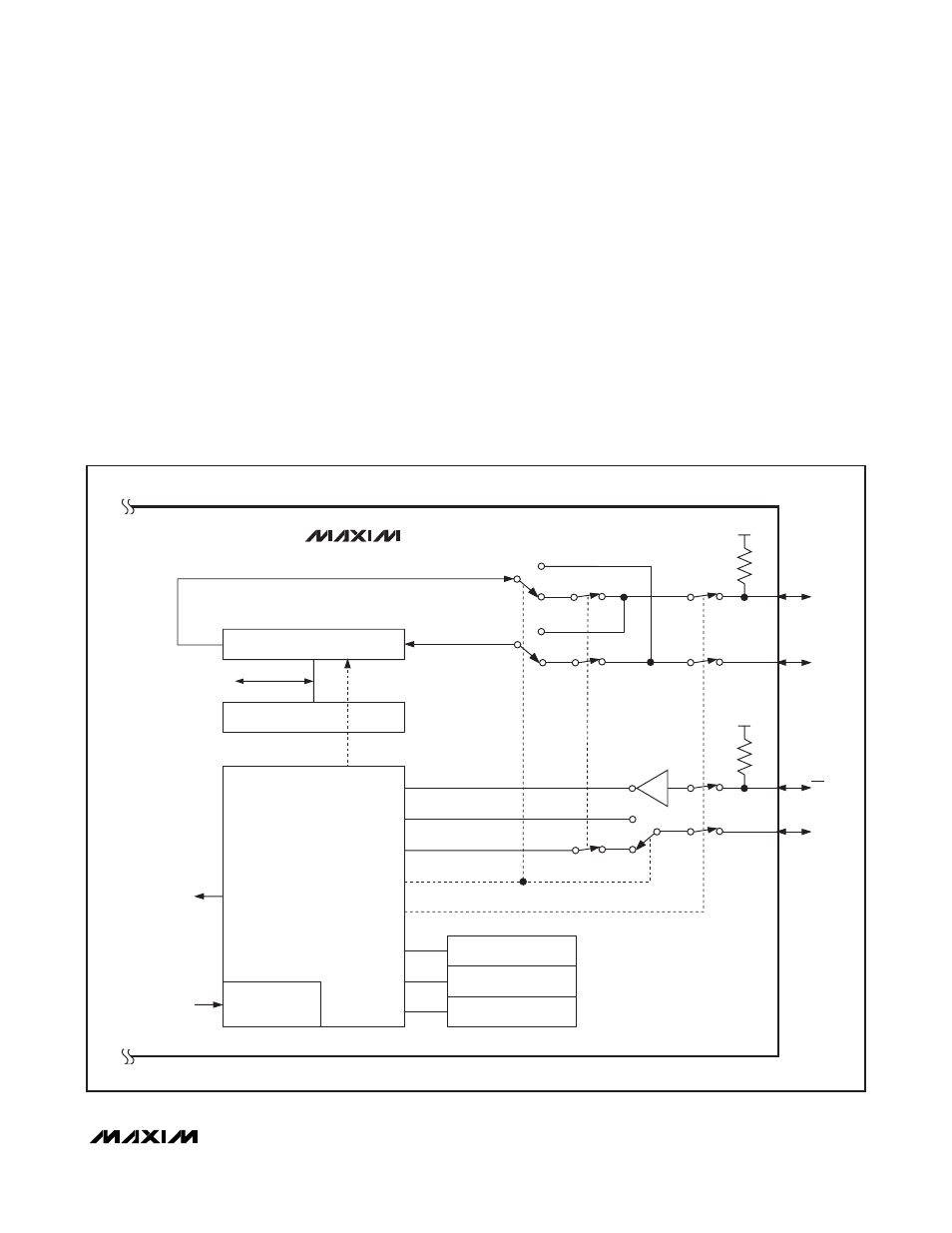
frequency is limited to SYSCLK/2 in master mode and
SYSCLK/8 in slave mode. Figure 10 shows the function-
al diagram of the SPI port. Figures 1 and 2 illustrate the
timing parameters listed in the
Electrical Characteristics
table.
General-Purpose Digital I/Os
The MAXQ7670 provides seven general-purpose digital
I/Os (GPIOs). Some of the GPIOs include an additional
special function (SF), such as a timer input/output. For
example, the state of P0.6/T0 is programmable to
depend on timer channel 0 logic. When used as a port,
each I/O is configurable for high-impedance, weak
pullup to DVDDIO or pulldown to GNDIO. At power-up,
each GPIO is configured as an input with a pullup to
DVDDIO. In addition, each GPIO can be programmed
to cause an interrupt (on falling or rising edges). In stop
mode, use any interrupt to wake-up the device.
The port direction (PD) register determines the
input/output direction of each I/O. The port output (PO)
register contains the current state of the logic output
buffers. When an I/O is configured as an output, writing
to the PO register controls the output logic state.
Reading the PO register shows the current state of the
output buffers, independent of the data direction. The
port input (PI) register is a read-only register that
always reflects the logic state of the I/Os.
SFR DATA BUS
READ BUFFER
SHIFT REGISTER
LSB(0)
MSB (15)
MISO
MASTER
SLAVE
SLAVE
SPI CONTROL UNIT
SYSCLK
SPI INTERRUPT
/2 MASTER (MAX)
/8 SLAVE (MAX)
SHIFT CLK
0
7
SPI CONTRL REG (SPICN)
SPI CONTRL REG (SPICF)
SPI CONTRL REG (SPICK)
MASTER/SLAVE SELECT
SCLK OUT
SCLK IN
SPI ENABLE
MASTER
MOSI
SCLK
DVDDIO
DVDDIO
SLAVE
MASTER
MAXQ7670
SS
Figure 10. SPI Functional Diagram