Detailed description – Rainbow Electronics MAXQ7670 User Manual
Page 17
MAXQ7670
Microcontroller with 10-Bit ADC,
PGA, 64KB Flash, and CAN Interface
______________________________________________________________________________________
17
Detailed Description
The MAXQ7670 incorporates a 16-bit RISC arithmetic
logic unit (ALU) with a Harvard memory architecture
that addresses 64KB (32K x 16) of flash and 2048
bytes (1024 x 16) of RAM memory. This core combined
with digital and analog peripherals provide versatile
data-acquisition functions. The peripherals include up to
seven digital I/Os, a 4-wire SPI interface, a CAN 2.0B
bus, a JTAG interface, a timer, an integrated RC oscilla-
tor, two linear regulators, a watchdog timer, three
power-supply supervisors, a 10-bit 250ksps SAR ADC
with programmable-gain amplifier (PGA) and eight sin-
gle-ended or four differential multiplexed inputs. The
power-efficient MAXQ20 µC core consumes less than
1mA/MIPS. Refer to the
MAXQ7670 User’s Guide
for
more detailed information on configuring and program-
ming the MAXQ7670.
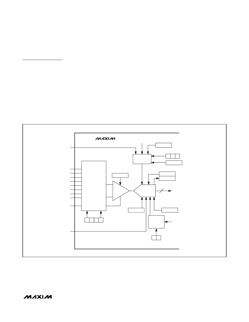
Analog Input Peripheral
The integrated 10-bit ADC employs an ultra-low-power
SAR-based conversion method and operates up to
250ksps with PGA = 1V/V (150.9ksps with PGA =
16V/V). The integrated 8-channel multiplexer (mux) and
PGA allow the ADC to measure eight single-ended (rel-
ative to AGND) or four fully differential analog inputs
with software-selectable input ranges through the PGA.
See Figures 3 and 4.
10-BIT ADC
250ksps
DATA
BUS
PGA
1V/V OR
16V/V
PGG
ADCE
1
0
ADCASD
ADCBY
ACTL
TIMER 0
ADCDUL
ADCRDY
ADCBIP
CONVERSION
CONTROL
ADC
CLOCK
DIV
8:1
MUX
ADCCD
1
0
3
2
ADCMX
1
2
0
10
ADCCLK
SOURCE
REFADC
P0.4/ADCCNV
AGND
AIN4
AIN3
AIN2
AIN7
AIN6
AIN5
AIN1
AIN0
MAXQ7670
Figure 3. Simplified Analog Input Diagram (Eight Single-Ended Inputs)