Rainbow Electronics MAXQ7670 User Manual
Page 20
MAXQ7670
Microcontroller with 10-Bit ADC,
PGA, 64KB Flash, and CAN Interface
20
______________________________________________________________________________________
Input Impedance
The input-capacitance charging rate determines the
time required for the T/H to acquire an input signal. The
required acquisition time lengthens with the increase of
the input signals source resistance. Any source below
5kΩ does not significantly affect the ADC’s perfor-
mance. A high-impedance source can be accommo-
dated by placing a 1µF capacitor between the input
channel and AGND. The combination of analog-input
source impedance and the capacitance at the analog
input creates an RC filter that limits the analog-input
bandwidth.
Controlling ADC Conversions
Use the following methods to control the ADC conver-
sion timing:
1) Software register bit control
2) Continuous conversion
3) Internal timer (T0)
4) External input through ADCCNV
Refer to the
MAXQ7670 User’s Guide
for more detailed
information on the ADC and mux.
POR and Brownout
The MAXQ7670 operates from a single, external +5V
supply connected to the DVDDIO. DVDDIO is the sup-
ply rail for the digital I/O and the supply input for both
integrated linear regulators. The +3.3V linear regulator
powers AVDD, while the +2.5V linear regulator powers
DVDD. Alternatively, connect REGEN2 to DVDDIO and
apply external power supplies to AVDD and DVDD.
Power supplies DVDDIO, DVDD, and AVDD each
include a brownout monitor that alerts the µC through
an interrupt when the corresponding supply voltages
drop below a defined threshold. This condition is gen-
erally referred to as brownout interrupt (BOI). Enable
BOI by setting the VABE, VDBE, and VIBE bits in the
APE register. By continually checking for low supply
voltages, appropriate action can be taken for brownout
conditions.
Startup Using Internal Regulators
Once the +5V DVDDIO supply reaches approximately
1.25V, the +2.5V linear regulator turns on and DVDD
begins ramping. Between the DVDD levels of 1V and
the reset threshold, the DVDD monitor holds RESET
low. DVDD releases RESET after reaching the reset
threshold. The MAXQ7670 jumps to the reset vector
location (8000h in the utility ROM). During this time,
DVDD finishes ramping to its nominal voltage of +2.5V.
During this POR time, the software-enabled +3.3V lin-
ear regulator remains off. Turn on the +3.3V linear regu-
lator after the MAXQ7670 has completed its bootup
routines and is running application code. To turn on the
+3.3V regulator, set the LRAPD bit in the APE register
to 0. The AVDD supply begins ramping to its nominal
voltage of +3.3V.
Brownout Detectors
The MAXQ7670 features brownout monitors for the +5V
DVDDIO, +3.3V AVDD, and +2.5V DVDD power sup-
plies. When enabled, these monitors generate interrupts
when DVDDIO, AVDD, or DVDD fall below their respec-
tive brownout thresholds. Monitoring the supply rails
alerts the µC to brownout conditions so appropriate
action can be taken. Under normal conditions the DVDDIO
brownout monitor signals a falling +5V supply before
the DVDD or AVDD brownout monitors indicate that the
+2.5V or +3.3V are falling. The exceptions to this condi-
tion are:
• If either DVDD or AVDD are externally powered and
the source of power is removed
• If there is some type of device failure that pulls the reg-
ulator outputs low without affecting the +5V DVDDIO
supply
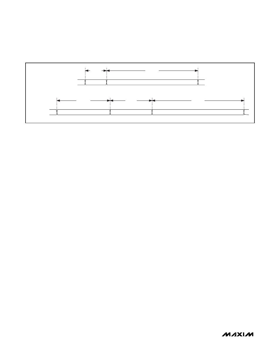
SAR CYCLE
PGA = 1V/V
SAR CYCLE
PGA = 16V/V
SAR TRACK
HOLD AND SAR CONVERT
PGA TRACK
PGA HOLD, SAR TRACK
HOLD AND SAR CONVERT
3 SCLK
13 SCLK
7.5 SCLK
6 SCLK
13 SCLK
Figure 5. Conversion Timing Differences Between Gain = 1V/V and Gain = 16V/V