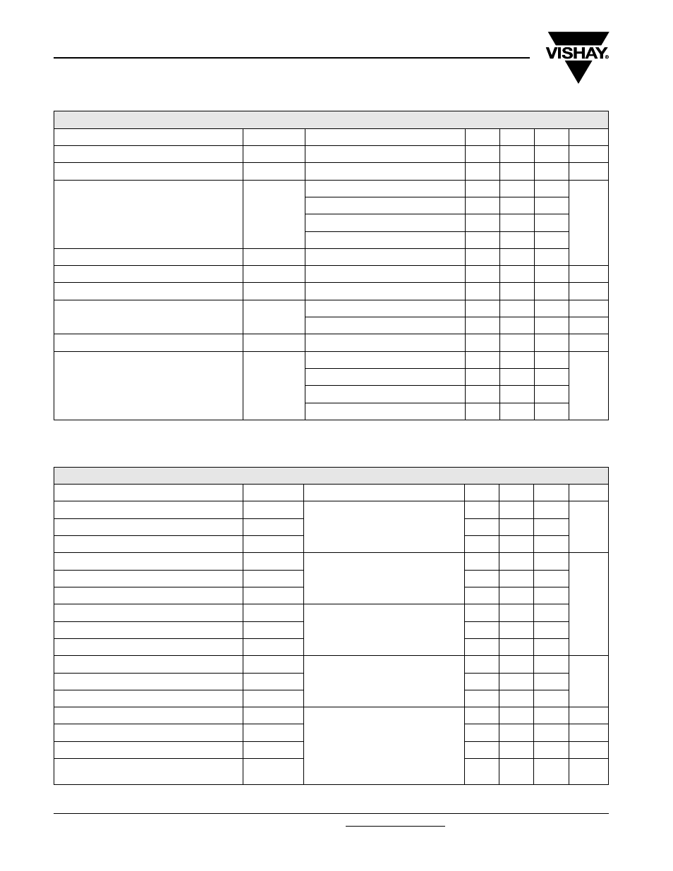
Vishay high power products, Full-bridge" igbt mtp (warp speed igbt), 50 a, Electrical specifications (t – C&H Technology 25MT060WFAPbF User Manual
Page 3: Switching characteristics (t, 25 °c unless otherwise specified)
www.vishay.com
For technical questions, contact: [email protected]
Document Number: 94539
2
Revision: 30-May-08
25MT060WFAPbF
Vishay High Power Products
"Full-Bridge" IGBT MTP
(Warp Speed IGBT), 50 A
Note
(1)
I
CES
includes also opposite leg overall leakage
ELECTRICAL SPECIFICATIONS (T
J
= 25 °C unless otherwise noted)
PARAMETER SYMBOL
TEST
CONDITIONS
MIN.
TYP.
MAX.
UNITS
Collector to emitter breakdown voltage
V
(BR)CES
V
GE
= 0 V, I
C
= 250 µA
600
-
-
V
Temperature coefficient of breakdown voltage
ΔV
(BR)CES
/
ΔT
J
V
GE
= 0 V, I
C
= 4 mA (25 to 125 °C)
-
+ 0.6
-
V/°C
Collector to emitter saturation voltage
V
CE(on)
V
GE
= 15 V, I
C
= 25 A
-
2.22
3.14
V
V
GE
= 15 V, I
C
= 50 A
-
2.43
3.25
V
GE
= 15 V, I
C
= 25 A, T
J
= 150 °C
-
1.65
1.93
V
GE
= 15 V, I
C
= 50 A, T
J
= 150 °C
-
2.08
2.45
Gate threshold voltage
V
GE(th)
V
CE
= V
GE
, I
C
= 250 µA
3
-
6
Temperature coefficient of threshold voltage
ΔV
GE(th)
/
ΔT
J
V
CE
= V
GE
, I
C
= 250 µA (25 to 125 °C)
-
- 17
-
mV/°C
Transconductance
g
fe
V
CE
= 100 V, I
C
= 25 A, PW = 80 µs
-
43
-
S
Zero gate voltage collector current
I
CES
(1)
V
GE
= 0 V, V
CE
= 600 V, T
J
= 25 °C
-
-
250
µA
V
GE
= 0 V, V
CE
= 600 V, T
J
= 150 °C
-
-
10
mA
Gate to emitter leakage current
I
GES
V
GE
= ± 20 V
-
-
± 250
nA
Diode forward voltage drop
V
FM
I
C
= 25 A
-
1.36
1.64
V
I
C
= 50 A
-
1.57
1.93
I
C
= 25 A; T
J
= 150 °C
-
1.19
1.42
I
C
= 50 A; T
J
= 150 °C
-
1.48
1.80
SWITCHING CHARACTERISTICS (T
J
= 25 °C unless otherwise specified)
PARAMETER SYMBOL
TEST
CONDITIONS
MIN.
TYP.
MAX.
UNITS
Total gate charge (turn-on)
Q
g
I
C
= 25 A
V
CC
= 480 V
V
GE
= 15 V
-
175
263
nC
Gate to emitter charge (turn-on)
Q
ge
-
27
41
Gate to collector charge (turn-on)
Q
gc
-
71
107
Turn-on switching loss
E
on
R
g
= 5
Ω, I
C
= 25 A
V
CC
= 480 V
V
GE
= ± 15 V
-
0.13
0.20
mJ
Turn-off switching loss
E
off
-
0.42
0.62
Total switching loss
E
tot
-
0.55
0.82
Turn-on switching loss
E
on
R
g
= 5
Ω, I
C
= 25 A
V
CC
= 480 V
V
GE
= ± 15 V, T
J
= 125 °C
-
0.39
0.59
Turn-off switching loss
E
off
-
0.49
0.74
Total switching loss
E
tot
-
0.88
1.32
Input capacitance
C
ies
V
GE
= 0 V
V
CC
= 30 V
f = 1.0 MHz
-
3610
5415
pF
Output capacitance
C
oes
-
714
1071
Reverse transfer capacitance
C
res
-
58
87
Diode reverse recovery time
t
rr
V
R
= 200 V;
I
C
= 25 A;
dI/dt = 200 A/µs
-
50
-
ns
Diode peak reverse current
I
rr
-
4.5
-
A
Diode Recovery charge
Q
rr
-
112
-
nC
Diode peakrate of fall of
recovery during t
b
dI
(rec)M
/dt
-
250
-
A/µs