Cpv363m4kpbf, Vishay semiconductors – C&H Technology CPV363M4KPbF User Manual
Page 4
CPV363M4KPbF
www.vishay.com
Vishay Semiconductors
Revision: 11-Jun-13
3
Document Number: 94485
For technical questions within your region:
,
,
THIS DOCUMENT IS SUBJECT TO CHANGE WITHOUT NOTICE. THE PRODUCTS DESCRIBED HEREIN AND THIS DOCUMENT
ARE SUBJECT TO SPECIFIC DISCLAIMERS, SET FORTH AT
www.vishay.com/doc?91000
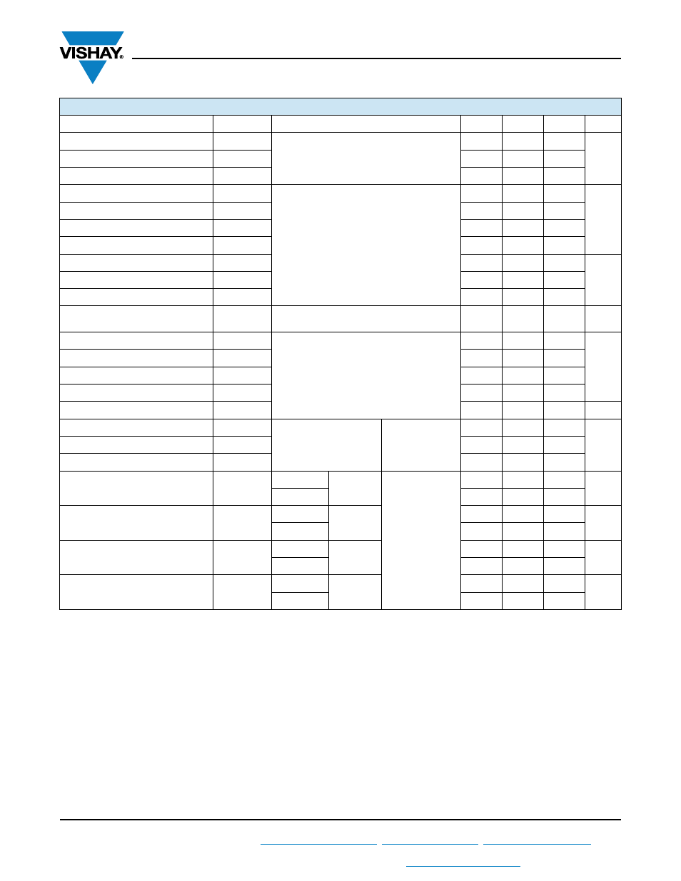
SWITCHING CHARACTERISTICS (T
J
= 25 °C unless otherwise specified)
PARAMETER SYMBOL
TEST
CONDITIONS
MIN.
TYP.
MAX.
UNITS
Total gate charge (turn-on)
Q
g
I
C
= 6 A
V
CC
= 400 V
See fig. 8
-
61
91
nC
Gate to emitter charge (turn-on)
Q
ge
-
7.4
11
Gate to collector charge (turn-on)
Q
gc
-
27
40
Turn-on delay time
t
d(on)
T
J
= 25 °C
I
C
= 6.0 A, V
CC
= 480 V
V
GE
= 15 V, R
G
= 23
Energy losses include “tail” and diode
reverse recovery
See fig. 9, 10, 18
-
55
-
ns
Rise time
t
r
-
24
-
Turn-off delay time
t
d(off)
-
107
160
Fall time
t
f
-
92
140
Turn-on switching loss
E
on
-
0.28
-
mJ
Turn-off switching loss
E
off
-
0.10
-
Total switching loss
E
ts
-
0.39
0.50
Short circuit withstand time
t
SC
V
CC
= 360 V, T
J
= 125 °C
V
GE
= 15 V, R
G
= 23
, V
CPK
< 500 V
10
-
-
μs
Turn-on delay time
t
d(on)
T
J
= 150 °C
I
C
= 6.0 A, V
CC
= 480 V
V
GE
= 15 V, R
G
= 23
Energy losses include “tail” and
diode reverse recovery
See fig. 10, 11, 18
-
54
-
ns
Rise time
t
r
-
24
-
Turn-off delay time
t
d(off)
-
161
-
Fall time
t
f
-
244
-
Total switching loss
E
ts
-
0.60
-
mJ
Input capacitance
C
ies
V
GE
= 0 V
V
CC
= 30 V
ƒ = 1.0 MHz
See fig. 7
-
740
-
pF
Output capacitance
C
oes
-
100
-
Reverse transfer capacitance
C
res
-
9.3
-
Diode reverse recovery time
t
rr
T
J
= 25 °C
See fig. 14
I
F
= 12 A
V
R
= 200 V
dI/dt = 200 A/μs
-
42
60
ns
T
J
= 125 °C
-
80
120
Diode peak reverse recovery
current
I
rr
T
J
= 25 °C
See fig. 15
-
3.5
6.0
A
T
J
= 125 °C
-
5.6
10
Diode reverse recovery charge
Q
rr
T
J
= 25 °C
See fig. 16
-
80
180
nC
T
J
= 125 °C
-
220
600
Diode peak rate of fall of recovery
during t
b
dI
(rec)M
/dt
T
J
= 25 °C
See fig. 17
-
180
-
A/μs
T
J
= 125 °C
-
120
-