Vishay high power products, Electrical characteristics (t, 25 °c unless otherwise specified) – C&H Technology GB200TS60NPbF User Manual
Page 3: Switching characteristics (t
www.vishay.com
For technical questions, contact: [email protected]
Document Number: 94503
2
Revision: 07-May-08
GB200TS60NPbF
Vishay High Power Products
INT-A-PAK "Half-Bridge"
(Ultrafast Speed IGBT),
209 A
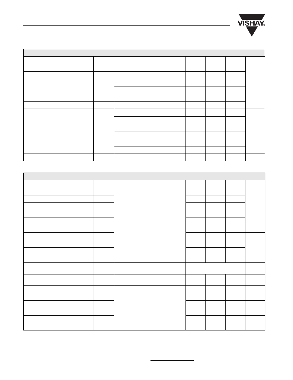
ELECTRICAL CHARACTERISTICS (T
J
= 25 °C unless otherwise specified)
PARAMETER SYMBOL
TEST
CONDITIONS
MIN.
TYP.
MAX.
UNITS
Collector to emitter breakdown voltage
V
BR(CES)
V
GE
= 0 V, I
C
= 500 µA
600
-
-
V
Collector to emitter voltage
V
CE(on)
V
GE
= 15 V, I
C
= 100 A
-
1.95
2.1
V
GE
= 15 V, I
C
= 200 A
-
2.6
2.84
V
GE
= 15 V, I
C
= 100 A, T
J
= 125 °C
-
2.28
2.5
V
GE
= 15 V, I
C
= 200 A, T
J
= 125 °C
-
3.14
3.48
Gate threshold voltage
V
GE(th)
V
CE
= V
GE
, I
C
= 500 µA
3
4.2
6
Collector to emitter leakage current
I
CES
V
GE
= 0 V, V
CE
= 600 V
-
0.005
0.2
mA
V
GE
= 0 V, V
CE
= 600 V, T
J
= 150 °C
-
0.01
15
Diode forward voltage drop
V
FM
I
C
= 100 A
-
1.39
1.78
V
I
C
= 200 A
-
1.64
2.2
I
C
= 100 A, T
J
= 125 °C
-
1.32
1.69
I
C
= 200 A, T
J
= 125 °C
-
1.67
2.30
Gate to emitter leakage current
I
GES
V
GE
= ± 20 V
-
-
± 200
nA
SWITCHING CHARACTERISTICS (T
J
= 25 °C unless otherwise specified)
PARAMETER SYMBOL
TEST
CONDITIONS
MIN.
TYP.
MAX.
UNITS
Turn-on switching loss
E
on
I
C
= 200 A, V
CC
= 360 V, V
GE
= 15 V,
R
G
= 10
Ω, L = 200 µH
-
3.65
-
mJ
Turn-off switching loss
E
off
-
6.9
-
Total switching loss
E
tot
-
10.55
-
Turn-on switching loss
E
on
I
C
= 200 A, V
CC
= 360 V, V
GE
= 15 V,
R
G
= 10
Ω, L = 200 µH, T
J
= 125 °C
-
3.8
-
Turn-off switching loss
E
off
-
7.8
-
Total switching loss
E
tot
-
11.6
-
Turn-on delay time
t
d(on)
-
507
-
ns
Rise time
t
r
-
133
-
Turn-off delay time
t
d(off)
-
538
-
Fall time
t
f
-
92
-
Reverse bias safe operating area
RBSOA
T
J
= 150 °C, I
C
= 400 A,
R
G
= 27
Ω, V
GE
= 15 V to 0
Fullsquare
Short circuit safe operating area
SCSOA
T
J
= 150 °C, V
CC
= 400 V, V
P
= 600 V,
R
G
= 27
Ω, V
GE
= 15 V to 0
10
-
-
Diode reverse recovery time
t
rr
I
F
= 50 A, dI
F
/dt = 200 A/µs,
V
CC
= 400 V, T
J
= 25 °C
-
226
260
ns
Diode peak reverse current
I
rr
-
17
20
A
Diode recovery charge
Q
rr
-
1900
2600
nC
Diode reverse recovery time
t
rr
I
F
= 50 A, dI
F
/dt = 200 A/µs,
V
CC
= 400 V, T
J
= 125 °C
-
290
330
ns
Diode peak reverse current
I
rr
-
25
30
A
Diode recovery charge
Q
rr
-
3600
5000
nC