Flat-base type insulated type, V(hold) i – C&H Technology PS11011 User Manual
Page 7
MITSUBISHI SEMICONDUCTOR
PS11011
FLAT-BASE TYPE
INSULATED TYPE
Jan. 2000
on
on
on
on
0
0
0
V
PN
DC-Bus voltage
Control voltage supply
Boot-strap voltage
N-Side input signal
P-Side input signal
Brake input signal
F
O
1 output signal
V
DB
V
CIN(N)
V
CIN(P)
V
CIN(Br)
F
OI
V
DH
b)
a)
PWM starts
R
U
P
,V
P
,W
P
,U
N
,V
N
,W
N
,Br
F
01
,F
02
,F
03
,CL
CU,CV,CW
GND(Logic)
ASIPM
5V
CPU
R
5.1k
Ω
10k
Ω
0.1nF
0.1nF
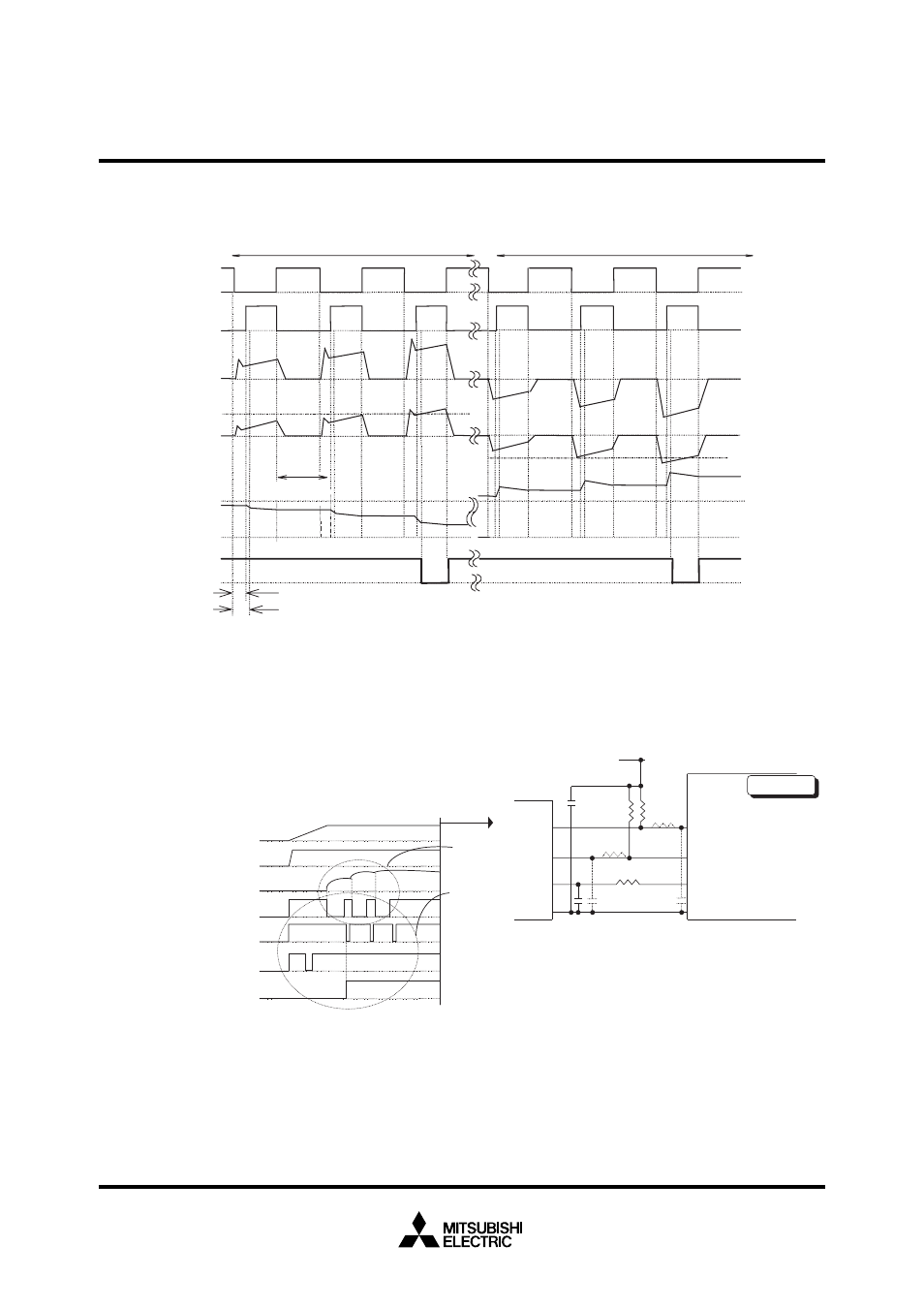
Fig. 8 INVERTER OUTPUT ANALOGUE CURRENT SENSING AND SIGNALING TIMING CHART
Fig. 10 RECOMMENDED I/O INTERFACE CIRCUIT
N-side IGBT Current
N-side FWDi Current
t(hold)
td(read)
Delay time
+I
CL
–I
CL
on
off
on
off
0
0
on
off
0
Ref
V
CIN
V(hold)
I
C
(V
S
)
V
C
V
CL
Fig. 9 START-UP SEQUENCE
Normally at start-up, Fo and CL output signals will be pulled-up
High to Supply voltage (OFF level); however, F
O1
output may fall to
Low (ON) level at the instant of the first ON input pulse to an N-Side
IGBT. This can happen particularly when the boot-strap capacitor is
of large size. F
O1
resetting sequence (together with the boot-strap
charging sequence) is explained in the following graph
a) Boot-strap charging scheme :
Apply a train of short ON pulses at all N-IGBT input pins for ad-
equate charging (pulse width = approx. 20
µ
s number of pulses =10
~ 500 depending on the boot-strap capacitor size)
b) F
O1
resetting sequence:
Apply ON signals to the following input pins : Br
→
Un/Vn/Wn
→
Up/Vp/Wp in that order.