Flat-base type insulated type – C&H Technology PS11011 User Manual
Page 6
MITSUBISHI SEMICONDUCTOR
PS11011
FLAT-BASE TYPE
INSULATED TYPE
Jan. 2000
S
C
delay time
Short circuit sensing signal V
S
Error output F
O1
Gate signal Vo of each phase
upper arm(ASIPM internal)
Input signal V
CIN
of each phase
upper arm
0V
0V
0V
0V
0V
0V
0V
0V
0V
Input signal V
CIN(p)
of each phase upper arm
Input signal V
CIN(n)
of each phase lower arm
Gate signal V
o(p)
of each phase upper arm
(ASIPM internal)
Gate signal V
o(n)
of each phase upper arm
(ASIPM internal)
Error output F
O1
V
CH
(5
µ
s)
V
CH
(505
µ
s)
0V
V
C
500
µ
s
r
CH
=
V
CH
(505
µ
s)-V
CH
(5
µ
s)
V
CH
(5
µ
s)
Note ; Ringing happens around the point where the signal output
voltage changes state from “analogue” to “data hold” due
to test circuit arrangement and instrumentational trouble.
Therefore, the rate of change is measured at a 5
µ
s delayed point.
200
–200
Analogue output signal
data hold range
1
2
3
4
5
400
300
100
0
–100
–300
–400
0
V
C
+(200%)
V
C0
V
C
–
(200%)
V
C
(V)
V
C
+
V
C
–
min
max
Real load current peak value.(%)(I
c
=I
o
✕
2)
V
DH
=15V
T
C
=
–
20
~
100˚C
(Fig. 4)
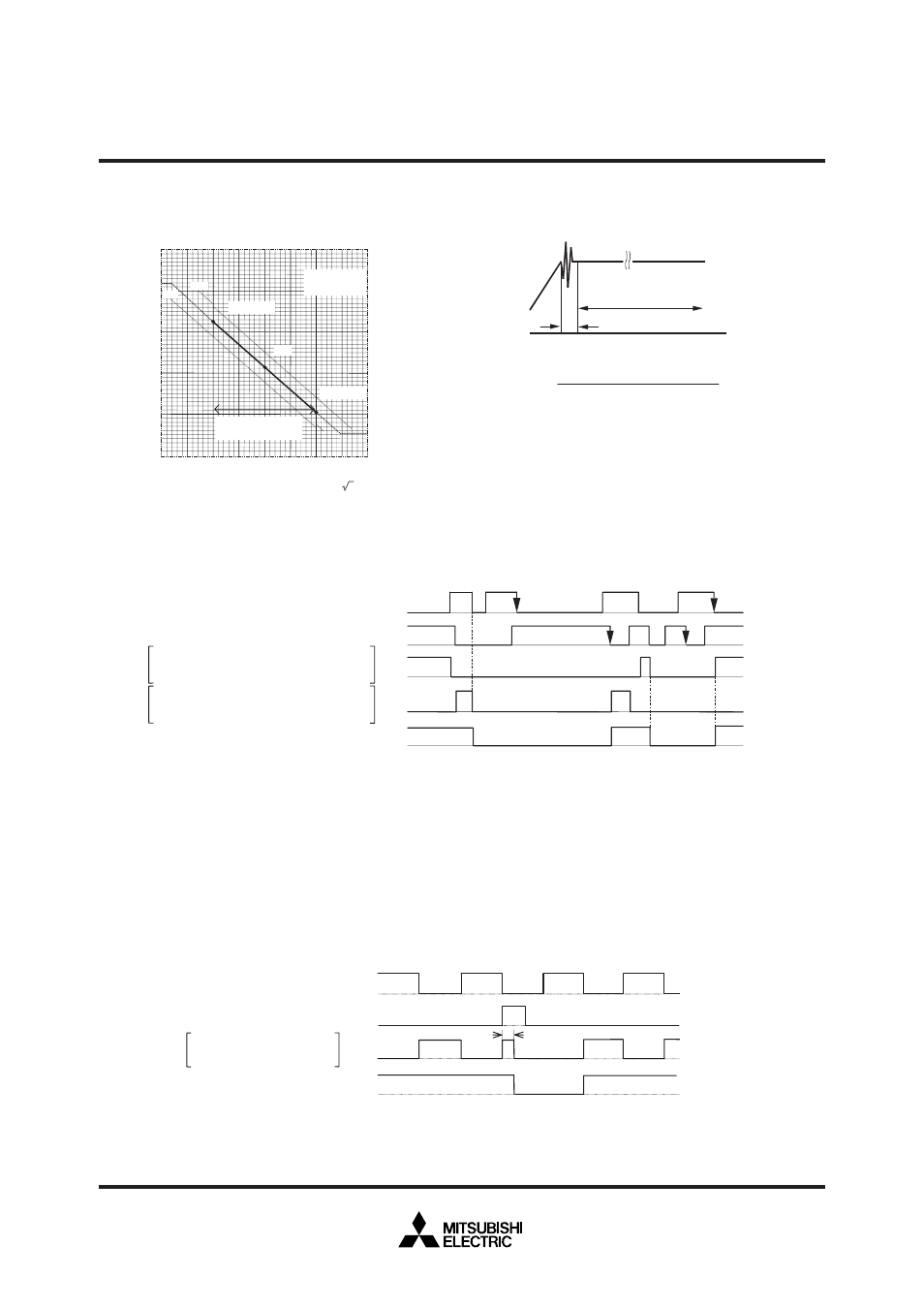
Fig. 4 OUTPUT CURRENT ANALOGUE SIGNALING
LINEARITY
Fig. 5 OUTPUT CURRENT ANALOGUE SIGNALING
“DATA HOLD” DEFINITION
Fig. 6 INPUT INTERLOCK OPERATION TIMING CHART
Note : Input interlock protection circuit ; It is operated when the input signals for any upper-arm / lower-arm pair of a phase are simulta-
neously in “LOW” level.
By this interlocking, both upper and lower IGBTs of this mal-triggered phase are cut off, and “F
O
” signal is outputted. After an “input
interlock” operation the circuit is latched. The “F
O
” is reset by the high-to-low going edge of either an upper-leg, or a lower-leg input,
whichever comes in later.
Fig. 7 TIMING CHART AND SHORT CIRCUIT PROTECTION OPERATION
Note : Short circuit protection operation. The protection operates with “F
O
” flag and reset on a pulse-by-pulse scheme. The protection by
gate shutdown is given only to the IGBT that senses an overload (excluding the IGBT for the “Brake”).