Flat-base type insulated type, Integrated functions and features, Package outlines – C&H Technology PS11011 User Manual
Page 2
MITSUBISHI SEMICONDUCTOR
PS11011
FLAT-BASE TYPE
INSULATED TYPE
Jan. 2000
PS11011
INTEGRATED FUNCTIONS AND FEATURES
• Converter bridge for 3 phase AC-to-DC power conversion.
• Circuit for dynamic braking of motor regenerative energy.
• 3-phase IGBT inver ter bridge configured by the latest 3rd.
generation IGBT and diode technology.
• Inverter output current capability I
O
(Note 1):
APPLICATION
Acoustic noise-less 0.1kW/AC200V class 3 phase inverter and other motor control applica-
tions
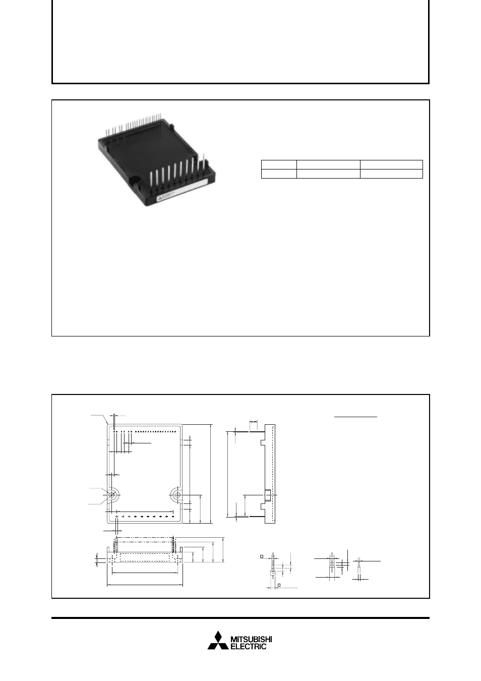
PACKAGE OUTLINES
MITSUBISHI SEMICONDUCTOR
PS11011
FLAT-BASE TYPE
INSULATED TYPE
INTEGRATED DRIVE, PROTECTION AND SYSTEM CONTROL FUNCTIONS:
• For inverter side upper-leg IGBTs : Drive circuit, High voltage isolated high-speed level shifting, Short circuit protection (SC).
Bootstrap circuit supply scheme (single drive power supply) and Under voltage protection (UV).
• For inverter side lower-leg IGBTs : Drive circuit, Short circuit protection (SC).
Control supply circuit under- & over- voltage protection (OV/UV).
System over temperature protection (OT). Fault output signaling circuit (F
O
) and Current limit warn-
ing signal output (CL).
• For Brake circuit IGBT : Drive circuit
• Warning and Fault signaling :
F
O1
: Short circuit protection for lower-leg IGBTs and Input interlocking against spurious arm shoot-through.
F
O2
: N-side control supply abnormality locking (OV/UV).
F
O3
: System over-temperature protection (OT).
CL : Warning for inverter current overload condition
• For system feedback control : Analogue signal feedback reproducing actual inverter output phase currents (3
φ
).
• Input Interface : 5V CMOS/TTL compatible, Schmitt trigger input, and Arm-Shoot-Through interlock protection.
(Note 1) : The inverter output current is assumed to be sinu-
soidal and the peak current value of each of the
above loading cases is defined as : I
OP
= I
O
×
√
2
(Fig. 1)
Type Name
PS11011
100% load
0.8A (rms)
150% over load
1.2A (rms), 1min
1 CBU+
2 CBU–
3 CBV+
4 CBV–
5 CBW+
6 CBW–
7 GND
8 NC
9 VDH
10 CL
11 FO1
12 FO2
13 FO3
14 CU
15 CV
16 CW
17 UP
18 VP
19 WP
20 UN
21 VN
22 WN
23 Br
31 R
32 S
33 T
34 P1
35 P2
36 N
37 B
38 U
39 V
40 W
2
±
0.3
54
±
0.5
0.5
±
0.03
0.8
0~0.8
0~0.8
0.4
0.5
62
±
1
20.4
±
1
27
±
1
84.2
±
1
72
±
0.8
17.6
±
0.5
5.08
±
0.3
✕
9 = 45.72
±
0.8
4-R2
2-R4
0.5
2
2
4.14
4
0.5
4
24
0.6
8.5
12
(12.25)
50
6
2
2 4
4
4
1 2 3 4
5 6
7 8 9101112131415161718192021 23
31
32
33
34
35
36
37
38
39
40
22
Terminals Assignment:
2-
φ
4
1.2
LABEL
3.5
✽
✽
✽
✽
Control Pin top
portion details
✽
Main terminal top
portion details
0.3
±
0.5
0
12
0.6
0.35MAX
±
0.5
0