Flat-base type insulated type – C&H Technology PS11011 User Manual
Page 3
MITSUBISHI SEMICONDUCTOR
PS11011
FLAT-BASE TYPE
INSULATED TYPE
Jan. 2000
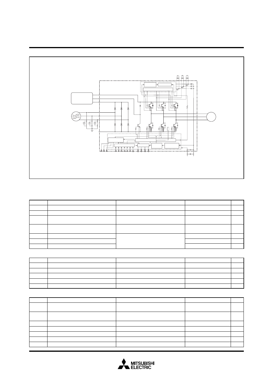
(15V line)
VDH
GND
CUCV CW
U
P
V
P
W
P
U
N
V
N
W
N
B
r
CL FO1 FO2 FO3
B
P2
P1
R
S
T
C
Z
N
M
W
V
U
AC200V line input
C3 ; 3.3
µ
F or more, tight tolerance, temp-compensated electrolytic type (Note : the value may change
depending on the type PWM control scheme used in the applied system)
C4 ; 2
µ
F R-category ceramic condenser for noise filtering.
C2 ;
3.3
µ
F or more
FO Logic
Protection
Circuit
Level shifter
Drive Circuit
Drive Curcuit
Trig signal conditioning
Current sensing
circuit
Protection
circuit
Control supply
fault sense
Z : Surge absorber.
C : AC filter (Ceramic condenser 2.2~6.5nF)
[Note : Additionally an appropriate Line-to line
surge absorber circuit maybe necessary
depending on the application environment].
AC 200V line
output
Brake resistor
connection,
Inrush prevention
circuit, etc.
Note 1) To prevent chances of signal oscillation, an RC coupling at each output is recommended. (see also Fig.10)
Note 2) By virtue of integrating an application specific type HVIC inside the module, direct coupling to CPU, without any opto or transformer isolation ispossible. (see also Fig.10)
Note 3) All these outputs are open collector type. Each signal line should be pulled up to plus side of the 5V power supply with approximately 5.1k
Ω
resistance. (see also Fig.10)
Note 4) The wiring between power DC link capacitor and P/N terminals should be as short as possible to protect the ASIPM against catastrophic high surge voltage. For extra
precaution, a small film type snubber capacitor (0.1~0.22
µ
F, high voltage type) is recommended to be mounted close to these P and N DC powerinput pins.
Analogue signal output corresponding to
each phase current (5V line) Note 1)
Each phase input (PWM)
(5V line) Note 2)
Fault output
(5V line) Note 3)
CBU–
CBU+
CBV–
CBV+
CBW–
CBW+
C4,C3
Application Specific Intelligent
Power Module
T.S.
C2
Each output IGBT collector current
Brake IGBT collector current
Brake diode anode current
INTERNAL FUNCTIONS BLOCK DIAGRAM
(Fig. 2)
V
V
450
500
Applied between P2-N
Applied between P2-N, Surge-value
Applied between P-U, V, W, Br or U, V, W,
Br-N
Applied between P-U, V, W, Br or U, V, W,
Br-N
T
C
= 25
°
C
Note: “( )” means I
C
peak value
Supply voltage
Supply voltage (surge)
V
CC
V
CC(surge)
Condition
Symbol
Item
Ratings
Unit
MAXIMUM RATINGS
(Tj = 25
°
C)
INVERTER PART (Including Brake Part)
V
P
or V
N
V
P(S)
or V
N(S)
±
I
C
(
±
I
CP
)
I
C
(I
CP
)
I
F
(I
FP
)
Each output IGBT collector-emitter static voltage
Each output IGBT collector-emitter
switching surge voltage
600
600
±
2 (
±
4)
2 (4)
2 (4)
V
V
A
A
A
V
20
Fault output supply voltage
Fault output current
Current-limit warning (CL) output voltage
CL output current
Analogue current signal output current
Applied between V
DH
-GND, C
BU+
-C
BU–
,
C
BV+
-C
BV–
, C
BW+
-C
BW–
Applied between U
P
· V
P
· W
P
· U
N
· V
N
·
W
N
· B
r
-GND
Applied between F
O1
· F
O2
· F
O3
-GND
Sink current of F
O1
· F
O2
· F
O3
Applied between CL-GND
Sink current of CL
Sink current of CU · CV · CW
V
DH
, V
DB
Supply voltage
Symbol
Item
Ratings
Unit
CONTROL PART
Condition
V
FO
I
FO
V
CL
I
CL
I
CO
V
CIN
Input signal voltage
–0.5 ~ 7.5
–0.5 ~ 7
15
–0.5 ~ 7
15
±
1
V
V
mA
V
mA
mA
3
φ
rectifying circuit
1 cycle at 60Hz, peak value non-repetitive
Value for one cycle of surge current
Condition
Symbol
Item
Ratings
Unit
V
RRM
Ea
I
O
I
FSM
I
2
t
Repetitive peak reverse voltage
Recommended AC input voltage
DC output current
Surge (non-repetitive) forward current
I
2
t for fusing
800
220
25
138
80
V
V
A
A
A
2
s
CONVERTER PART