Vs-gb90da60u, Vishay semiconductors, Thermal and mechanical specifications – C&H Technology VS-GB90DA60U User Manual
Page 4
VS-GB90DA60U
www.vishay.com
Vishay Semiconductors
Revision: 19-Sep-12
3
Document Number: 94771
For technical questions within your region:
,
,
THIS DOCUMENT IS SUBJECT TO CHANGE WITHOUT NOTICE. THE PRODUCTS DESCRIBED HEREIN AND THIS DOCUMENT
ARE SUBJECT TO SPECIFIC DISCLAIMERS, SET FORTH AT
www.vishay.com/doc?91000
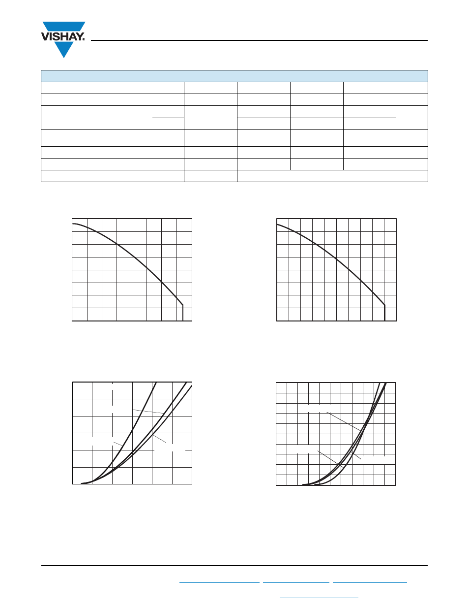
Fig. 1 - Maximum DC IGBT Collector Current vs.
Case Temperature
Fig. 2 - Typical Collector to Emitter Voltage (V)
Fig. 3 - Maximum Allowable Forward Current vs.
Case Temperature, Diode Leg
Fig. 4 - Typical Forward Voltage Drop Characteristics
THERMAL AND MECHANICAL SPECIFICATIONS
PARAMETER
SYMBOL
MIN. TYP. MAX.
UNITS
Maximum junction and storage temperature
T
J
, T
Stg
- 40
-
150
°C
Junction to case
IGBT
R
thJC
-
-
0.20
°C/W
Diode
-
-
0.33
Case to sink thermal resistance, flat greased
surface
R
thCS
-
0.1
-
Mounting torque, on termianls and heatsink
T
-
-
1.3
Nm
Weight
-
30
-
g
Case style
SOT-227
I
C
-
Continuous Collector Current (A)
Allowable Case Temperature (°C)
0 20 40 60 80 100 120 140 160
0
20
40
60
80
100
120
140
160
DC
V
CE
-
Collector-to-Emitter Voltage (V)
I
C
-
Collector to Emitter Curr
ent (A)
0.0
1.0
2.0
3.0
4.0
5.0
6.0
0
200
100
50
150
250
300
V
GE
= 15V
T
J
= 150 °C
T
J
= 125 °C
T
J
= 25 °C
I
F
-
Continuous Forward Current (A)
Allowable Case Temperature (°C)
0 20 40 60 80 100 120 140 160 180 200
0
20
40
60
80
100
120
140
160
V
F
-
Forward Voltage Drop (V)
I
F
- Forwar
d
Curr
ent (A)
0 0.2 0.4 0.6 0.8 1.0 1.2 1.4 1.6 1.8 2.0 2.2
0
40
80
120
160
200
T
J
= 25 °C
T
J
= 125 °C
T
J
= 150 °C