Section 3, Programming, Introduction – VXI TECHNOLOGY SVM2608 User Manual
Page 27: Device memory maps, Function offset, Register offset, Ection, Rogramming
www.vxitech.com
SVM2608 Preparation for Use
27
S
ECTION
3
P
ROGRAMMING
I
NTRODUCTION
The SVM2608 modules are VMEbus register-based devices for high-speed D16 or D32 data
retrieval. Register-based programming is a series of reads and writes directly to the module
registers. This eliminates the time for command parsing thus increasing speed.
D
EVICE
M
EMORY
M
APS
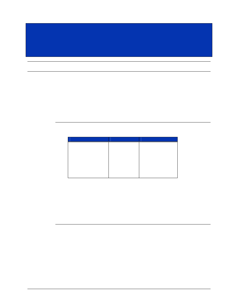
Function Offset
The function offset helps define where in A32 space a WRITE or READ operation is performed.
The offsets are defined as follows:
Function
Decimal Value
Hexadecimal Value
CH0 Data
0
0x000000
CH1 Data
2097152
0x200000
CH2 Data
4194304
0x400000
CH3 Data
6291456
0x600000
CH4 (Option -01)
8388608
0x800000
CH5 (Option -01)
10485760
0xA00000
Registers 12582912
0xC00000
Reserved 14680064
0xE00000
CH0 – 5 Data
These addresses are used to store data.
Registers
These addresses are the A32 memory registers. They are used to program the
settings for each channel, collect FIFO data, collect results or sent commands
to the microprocessor.
Reserved
These addresses are reserved for future use.
Register Offset
The register offset is located within the module's A32 address space. When data is sent to a
register address, the address that is written to is the sum of the module base address, the function
offset and the register offset:
Register Address = Module Base Address + Function Offset + Register Offset
Table 3-1 shows the A32 map of the SVM2608 registers.