6 write (wrt) command, 5 memory width and byte alignment – Texas Instruments DM648 DSP User Manual
Page 18
www.ti.com
2.4.6
Write (WRT) Command
DDR_D[31:0]
DDR_DQS[3:0]
COL
BANK
DQM7
Sample
D0
D1
D2
D3
D4
D5
D6
D7
DQM1 DQM2 DQM3 DQM4 DQM5 DQM6
DQM8
Write Latency
DDR_A[10]
DDR_CLK
DDR_CLK
DDR_CS
DDR_CKE
DDR_RAS
DDR_WE
DDR_DQM[3:0]
DDR_CAS
DDR_BA[2:0]
DDR_A[13:0]
2.5
Memory Width and Byte Alignment
Peripheral Architecture
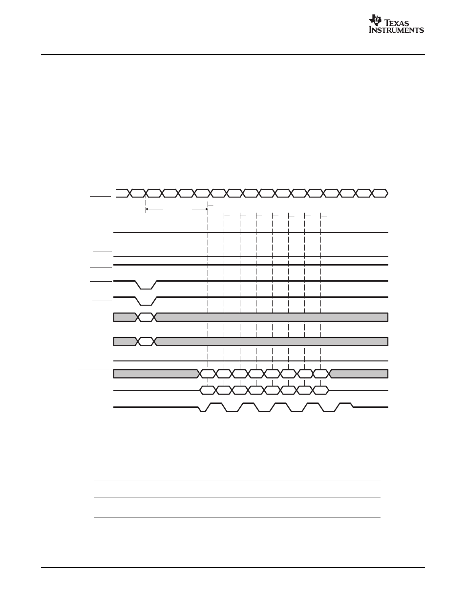
Prior to a WRT command, the desired bank and row are activated by the ACTV command. Following the
WRT command, a write latency is incurred. Write latency is equal to CAS latency minus 1. All writes have
a burst length of 8. The use of the DDR_DQM outputs allows byte and halfword writes to be executed.
shows the timing for a write on the DDR2 memory controller.
If the transfer request is for less than 8 words, depending on the scheduling result and the pending
commands, the DDR2 memory controller can:
•
Mask out the additional data using DDR_DQM outputs
•
Terminate the write burst and start a new write burst
The DDR2 memory controller does not perform the DEAC command until page information becomes
invalid.
Figure 9. DDR2 WRT Command
The DDR2 memory controller supports memory widths of 16 bits and 32 bits.
summarizes the
addressable memory ranges on the DDR2 memory controller.
Table 4. Addressable Memory Ranges
Memory Width
Maximum Addressable Bytes
Address Type Generated by DDR2
Memory Controller
×
16
128 Mbytes
Halfword address
×
32
256 Mbytes
Word address
DSP DDR2 Memory Controller
18
SPRUEK5A – October 2007