4 protocol description(s), Table 3. truth table for ddr2 sdram commands, Peripheral architecture – Texas Instruments DM648 DSP User Manual
Page 13

www.ti.com
2.4
Protocol Description(s)
Peripheral Architecture
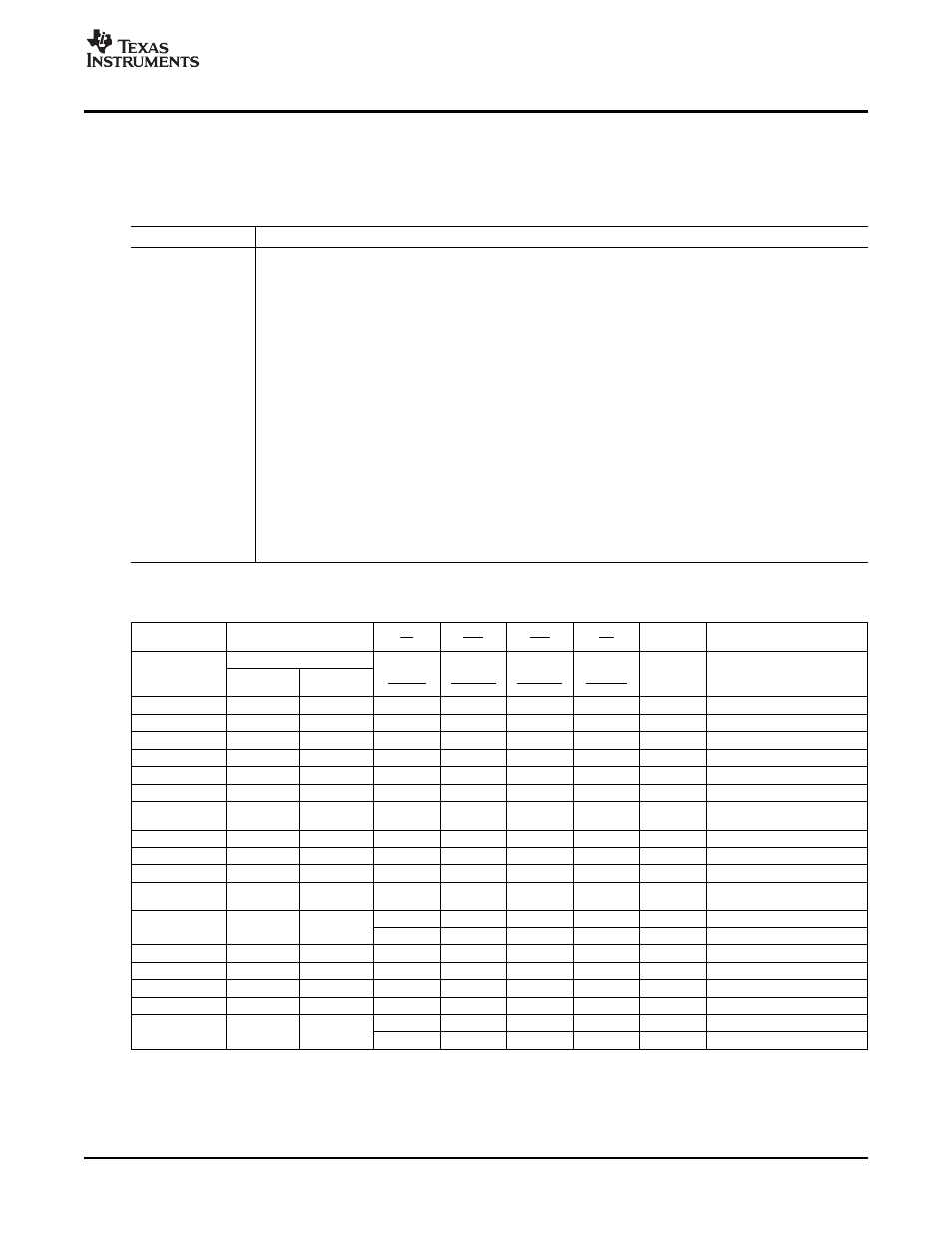
The DDR2 memory controller supports the DDR2 SDRAM commands listed in
.
shows the
signal truth table for the DDR2 SDRAM commands.
Table 2. DDR2 SDRAM Commands
Command
Function
ACTV
Activates the selected bank and row.
DCAB
Precharge all command. Deactivates (precharges) all banks.
DEAC
Precharge single command. Deactivates (precharges) a single bank.
DESEL
Device Deselect.
EMRS
Extended Mode Register set. Allows altering the contents of the mode register.
MRS
Mode register set. Allows altering the contents of the mode register.
NOP
No operation.
Power Down
Power down mode.
READ
Inputs the starting column address and begins the read operation.
READ with
Inputs the starting column address and begins the read operation. The read operation is followed by a
autoprecharge
precharge.
REFR
Autorefresh cycle.
SLFREFR
Self-refresh mode.
WRT
Inputs the starting column address and begins the write operation.
WRT with
Inputs the starting column address and begins the write operation. The write operation is followed by a
autoprecharge
precharge.
Table 3. Truth Table for DDR2 SDRAM Commands
DDR2 SDRAM
Signals
CKE
CS
RAS
CAS
WE
BA[2:0]
A[13:11, 9:0]
A10
DDR_CKE
DDR2 Memory
Previous
DDR_BA[2:0
Controller Signals
Cycles
Current Cycle
DDR_CS
DDR_RAS
DDR_CAS
DDR_WE
]
DDR_A[13:11, 9:0]
DDR_A[10]
ACTV
H
(1)
H
L
L
H
H
Bank
Row Address
DCAB
H
H
L
L
H
L
X
X
L
DEAC
H
H
L
L
H
L
Bank
X
L
MRS
H
H
L
L
L
L
BA
(2)
OP Code
EMRS
H
H
L
L
L
L
BA
OP Code
READ
H
H
L
H
L
H
BA
Column Address
L
READ with
H
H
L
H
L
H
BA
Column Address
H
precharge
WRT
H
H
L
H
L
L
BA
Column Address
L
WRT with precharge
H
H
L
H
L
L
BA
Column Address
L
REFR
H
H
L
L
L
H
X
X
X
SLFREFR
H
L
L
L
L
H
X
X
X
entry
SLFREFR
L
H
H
X
X
X
X
X
X
exit
L
H
H
H
X
X
X
NOP
H
X
L
H
H
H
X
X
X
DESEL
H
X
H
X
X
X
X
X
X
Power Down entry
H
L
H
X
X
X
X
X
X
L
H
H
H
X
X
X
Power Down exit
L
H
H
X
X
X
X
X
X
L
H
H
H
X
X
X
(1)
Legend: H means logic high; L means logic low; X means don't care (either H or L).
(2)
BA refers to the bank address pins (BA[2:0]).
SPRUEK5A – October 2007
DSP DDR2 Memory Controller
13
