Transcend Information CompactFlash CF 300X User Manual
Page 36
T
T
T
S
S
S
2
2
2
G
G
G
~
~
~
1
1
1
6
6
6
G
G
G
C
C
C
F
F
F
3
3
3
0
0
0
0
0
0
300X CompactFlash Card
Transcend Information Inc.
V1.1
36
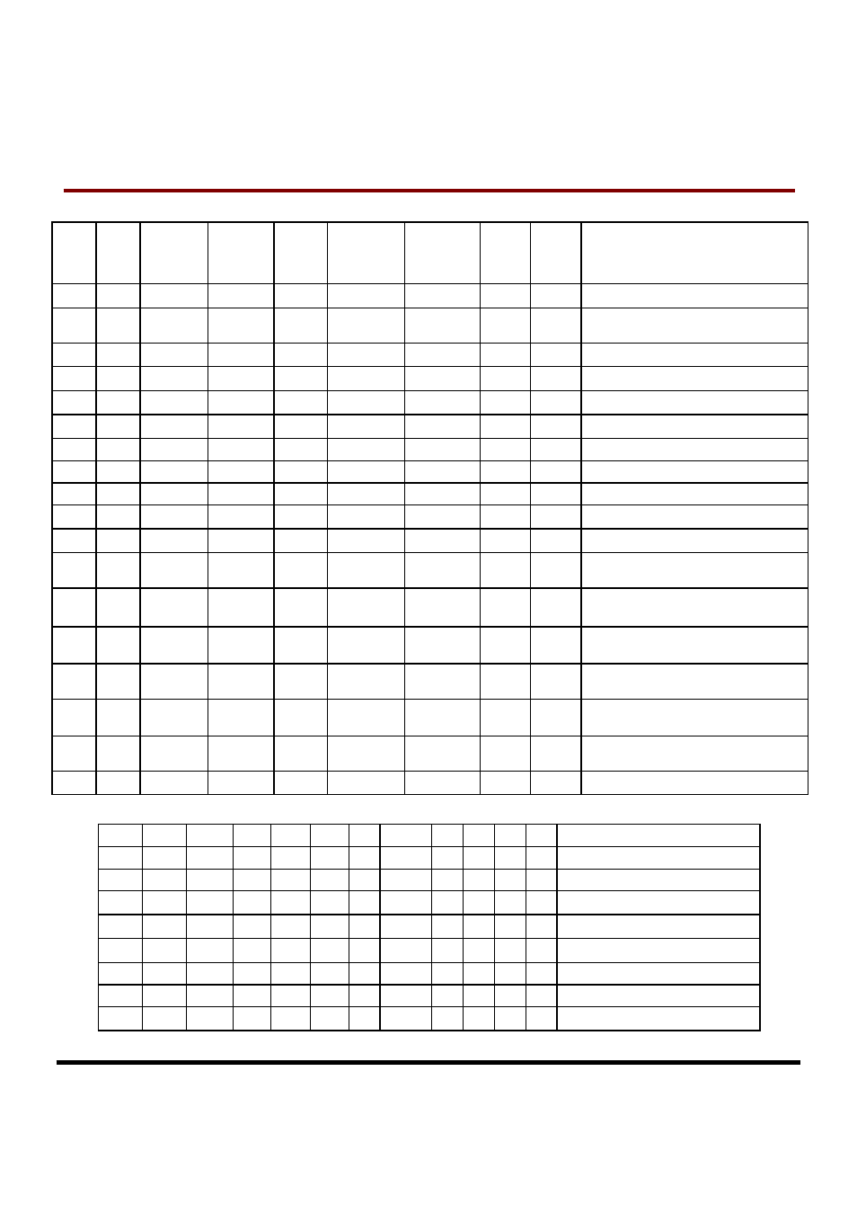
Table: PC Card Memory Mode UDMA Function
-CE2 -CE1
-DMARQ
-INPACK
-DMACK
-REG
STOP
-IOW
R
-DMARDY
-IORD
(R)-WAIT
(W)
STROBE
-WAIT
(R)-IORD
(W)
DMA
CMD
A10-
A00
Operation
1
1
1
X
X
X
X
No
XX
Standby
X
X
0
1
X
X
1
YES
XX
Device UDMA Transfer Request
(Assert DMARQ)
X
X
0
1
1
X
1
YES
XX
Host Acknowledge Preparation
1
1
0
1
1
1
1
YES
Static Host Acknowledge Preparation
1
1
0
0
1
1
1
YES
Static DMA Acknowledge (Stopped)
1
1
0
0
0
0
1
YES
Static Burst Initiation / Active
1
1
0
0
0
X
/ or \
YES
Static Burst Transfer
1
1
0
0
0
1
0 or 1
RD
Static Data In Burst Host Pause
1
1
0
0
0
0
0 or 1
RD
Static Data In Burst Device Pause
1
1
0
0
0
1
0 or 1
WR
Static Data Out Burst Device Pause
1
1
0
0
0
0
0 or 1
WR
Static Data Out Burst Host Pause
1
1
1
0
0
0
0 or 1
RD
Static Device Initiating BurstTermination
1
1
1
0
1
1
0 or 1
RD
Static
Host Acknowledement of Device
Initiated Burst Termination
1
1
0
0
1
0
0 or 1
YES
Static Host Initiating BurstTermination
1
1
1
0
1
1
0 or 1
YES
Static
Device Acknowledging Host Initiated
Burst Termination
1
1
1
0
1
1
/
YES
Static
Device Aligning STROBE to Asserted
before CRC Transfer
1
1
1
/
1
1
1
YES
Static CRC Data Transfer for UDMA Burst
1
1
1
1
1
1
1
YES
Static Burst Completed
Table: CompactFlash Storage Card Configuration Registers Decoding
-CE2 -CE1 -REG -OE -WE A10 A9 A8-A4 A3 A2 A1 A0 SELECTED REGISTER
X
0
0
0
1
0
1
00
0
0
0
0
Configuration Option Reg Read
X
0
0
1
0
0
1
00
0
0
0
0
Configuration Option Reg Write
X
0
0
0
1
0
1
00
0
0
1
0
Card Status Register Read
X
0
0
1
0
0
1
00
0
0
1
0
Card Status Register Write
X
0
0
0
1
0
1
00
0
1
0
0
Pin Replacement Register Read
X
0
0
1
0
0
1
00
0
1
0
0
Pin Replacement Register Write
X
0
0
0
1
0
1
00
0
1
1
0
Socket and Copy Register Read
X
0
0
1
0
0
1
00
0
1
1
0
Socket and Copy Register Write