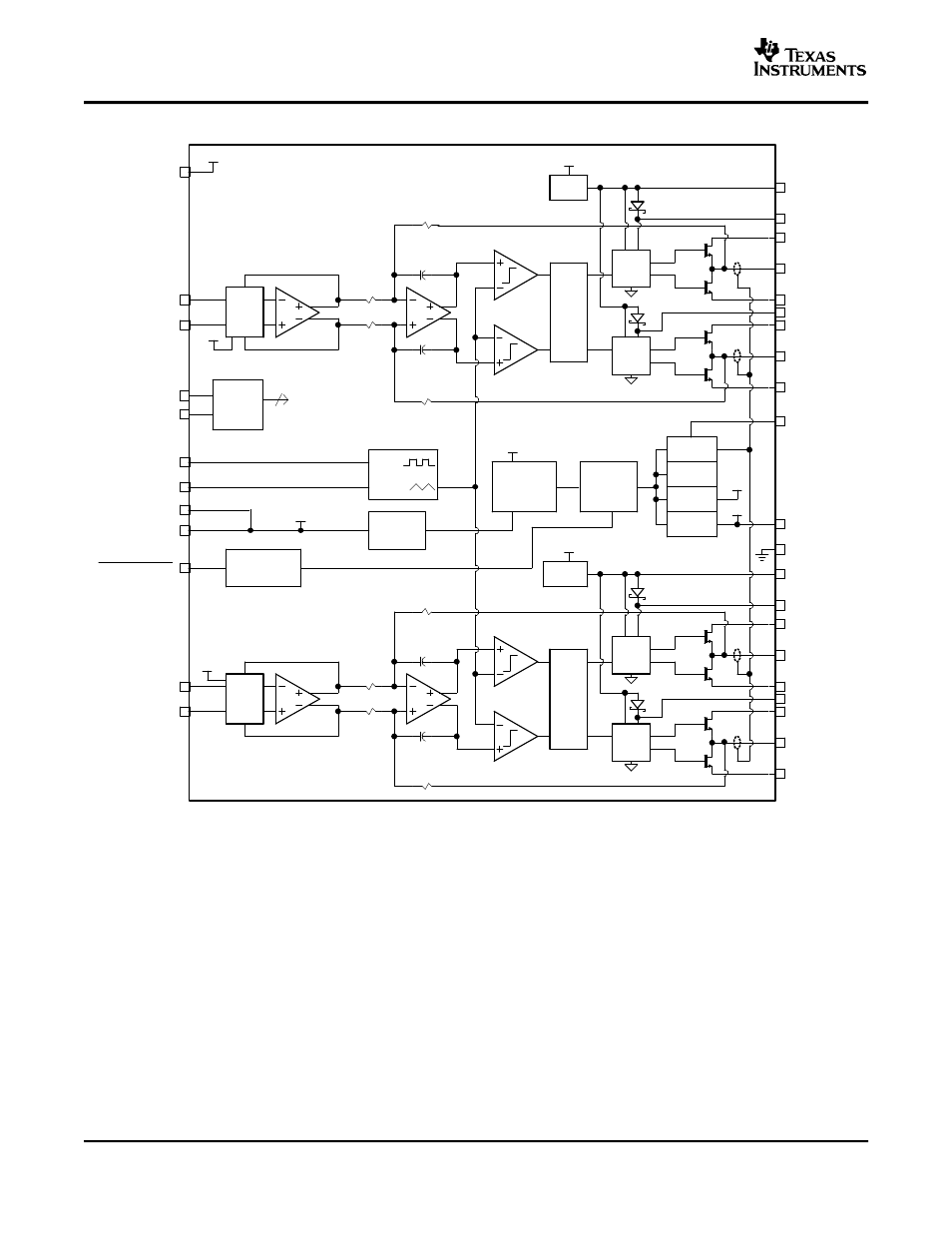
Functional block diagram – Texas Instruments TPA3008D2 User Manual
Page 4
www.ti.com
Biases
and
References
TTL Input
Buffer
(VCC Compl)
Start-up and
Protection
Logic
SC
Detect
Thermal
VDDok
RINP
RINN
Ramp
Generator
COSC
ROSC
VCCok
5-V LDO
AVCC
AVDD
AVDD
VDD
and
PWM
Mode
Logic
Gain
Adj.
Gain
Control
Deglitch
and
PWM
Mode
Logic
Gain
Adj.
LINP
LINN
Gate
Drive
VClamp
Gen
Gate
Drive
PVCC
BSRP
PVCCR(2)
ROUTP(2)
PGNDR
PGNDR
ROUTN(2)
PVCCR(2)
BSRN
Gate
Drive
VClamp
Gen
Gate
Drive
PVCC
BSLP
PVCCL(2)
LOUTP(2)
PGNDL
PGNDL
LOUTN(2)
PVCCL(2)
BSLN
VCLAMPL
VCLAMPR
GAIN0
4
To Gain Adj.
Blocks and
Start-up Logic
SHUTDOWN
V2P5
V2P5
V2P5
AVCC
AGND(2)
V2P5
V2P5
Deglitch
GAIN1
AV
DD
REF
FAULT
TPA3008D2
SLOS435A – MAY 2004 – REVISED JULY 2004
FUNCTIONAL BLOCK DIAGRAM
4
See also other documents in the category Texas Instruments Receivers and Amplifiers:
- THS4151 (26 pages)
- TRF1500 (74 pages)
- SLOU082 (28 pages)
- TAS5508-5121K8EVM (24 pages)
- TPA6102A2 (16 pages)
- TPA3001D1EVM (22 pages)
- TPA6030A4 (25 pages)
- TPA701 (26 pages)
- TPA6110A2 MSOP (18 pages)
- TAS5727 (21 pages)
- THS4503EVM (28 pages)
- TPA005D02 (50 pages)
- SLOU121 (42 pages)
- TPA0243 (20 pages)
- TPA0253 (20 pages)
- TPA102 MSOP (26 pages)
- THS4131 (26 pages)
- SLOU020A (28 pages)
- TPA751 MSOP (20 pages)
- TPA005D12 (44 pages)
- TPA6139A2 EVM (8 pages)
- TPA0103 (32 pages)
- SLOU106 (26 pages)
- THS4141 (26 pages)
- THS3001 (20 pages)
- TPA0233 (20 pages)
- TPA2008D2 (26 pages)
- 2004 (20 pages)
- TPA3003D2 (36 pages)
- SLAU081 (44 pages)
- TPA301 (28 pages)
- TPA3100D2 (11 pages)
- SLOU023A (26 pages)
- TAS5110D6REF (45 pages)
- TA5704EVM (27 pages)
- TAS5518 (20 pages)
- APA100 (42 pages)
- TPA3200D1 (30 pages)
- TAS5066PAG (22 pages)
- TPA6204A1 (16 pages)
- THS4150 (26 pages)
- TPA311 (28 pages)
- TPA6101A2 (16 pages)