Gain setting via gain0 and gain1 inputs, Input resistance, Application information (continued) – Texas Instruments TPA3008D2 User Manual
Page 16
www.ti.com
0.1
µ
F
0.1
µ
F
0.47
µ
F
33
µ
H
33
µ
H
OUTP
OUTN
L
1
L
2
C
1
C
2
C
3
1 nF
Ferrite
Chip Bead
OUTP
OUTN
Ferrite
Chip Bead
1 nF
Gain setting via GAIN0 and GAIN1 inputs
INPUT RESISTANCE
TPA3008D2
SLOS435A – MAY 2004 – REVISED JULY 2004
APPLICATION INFORMATION (continued)
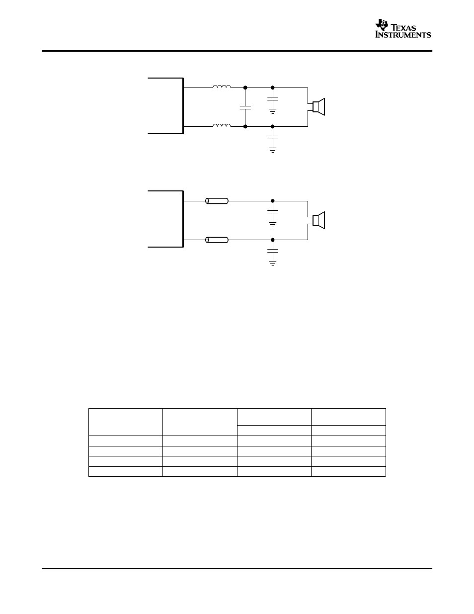
Figure 19. Typical LC Output Filter, Cutoff Frequency of 27 kHz, Speaker Impedance = 8
Ω
Figure 20. Typical Ferrite Chip Bead Filter (Chip bead example: Fair-Rite 2512067007Y3)
The gain of the TPA3008D2 is set by two input terminals, GAIN0 and GAIN1.
The gains listed in Table 1 are realized by changing the taps on the input resistors inside the amplifier. This
causes the input impedance (Z
i
) to be dependent on the gain setting. The actual gain settings are controlled by
ratios of resistors, so the gain variation from part-to-part is small. However, the input impedance may shift by
20% due to shifts in the actual resistance of the input resistors.
For design purposes, the input network (discussed in the next section) should be designed assuming an input
impedance of 26 k
Ω
, which is the absolute minimum input impedance of the TPA3008D2. At the lower gain
settings, the input impedance could increase as high as 165 k
Ω
Table 1. Gain Setting
INPUT IMPEDANCE
AMPLIFIER GAIN (dB)
(k
Ω
)
GAIN1
GAIN0
TYP
TYP
0
0
15.3
137
0
1
21.2
88
1
0
27.2
52
1
1
31.8
33
Each gain setting is achieved by varying the input resistance of the amplifier that can range from its smallest
value, 33 k
Ω
, to the largest value, 137 k
Ω
. As a result, if a single capacitor is used in the input high-pass filter,
the -3 dB or cutoff frequency changes when changing gain steps.
16