C controlled register bit map (cont.) – Renesas HD151TS207SS User Manual
Page 18
HD151TS207SS
Rev.1.00, Apr.25.2003, page 18 of 38
I
2
C Controlled Register Bit Map (cont.)
Byte18 Control Register
Bit
Description
Contents
Type
Default
Note
7
VCO2 Frequency Control Bit7
R/W
0
6
VCO2 Frequency Control Bit6
R/W
0
5
VCO2 Frequency Control Bit5
R/W
0
4
VCO2 Frequency Control Bit4
These bits are 10MHz digit of
VCO2 frequency.
0000 = 0, 0001 = 1 …. 1001 = 9
R/W
0
3
VCO2 Frequency Control Bit3
R/W
0
2
VCO2 Frequency Control Bit2
R/W
0
1
VCO2 Frequency Control Bit1
R/W
0
0
VCO2 Frequency Control Bit0
These bits are 1MHz digit of
VCO2 frequency.
0000 = 0, 0001 = 1 …. 1001 = 9
R/W
0
See
Note
1
Note:
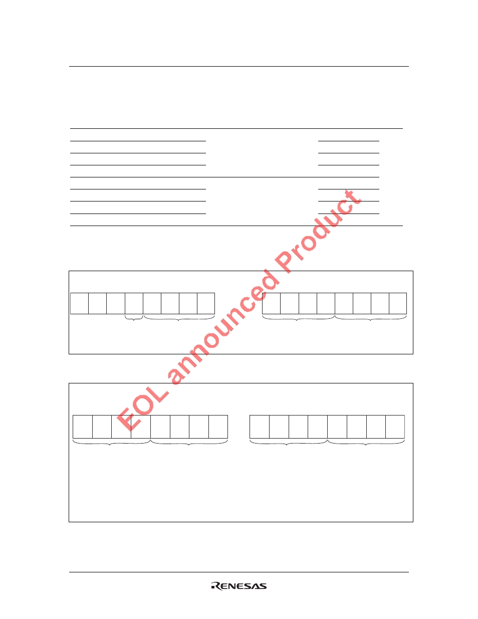
1. B17[3:0] and B18[7:0] must be written together (at writing B18) in every case.
How to set VCO2 frequency to 666 MHz.
0
0
0
1
0
1
1
0
ON
Write
Byte17
6
0
1
1
0
0
1
1
0
Byte18
6
6
max 720
min 200
How to read actual frequency of VCO2 and CPU clock
0
1
1
0
1
0
0
0
Byte20
8
6
0
1
1
0
0
1
1
0
Byte17[4] = 1
Actual VCO2 freq. read back.
Byte19
6
6
Note:
Case of VCO2 = 666.8 MHz.
Other clock frequency are able to read using the same way as shown at upper.
Byte19, Byte20 = Read back of VCO2 actual frequency.
Byte21, Byte22 = Read back of CPU actual frequency.