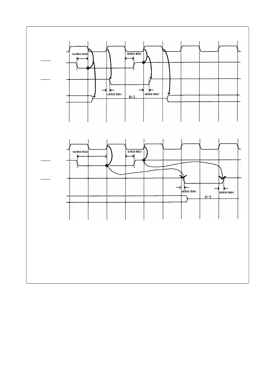
Figure 5.5 timing requirements – Renesas Emulation Pod M306V2T-RPD-E User Manual
Page 56
( 54 / 72 )
Figure 5.5 Timing requirements
Common to "with wait" and "no-wait" (actual MCU)
BCLK
Common to "with wait" and "no-wait" (this product)
BCLK
Note 1. P0
0
to P5
2
will be high-impedance regardless of the input level of BYTE pin and ports P4
0
to P4
3
function
selection bit (PM06) of the processor mode register 0.
Note 2. This product will be high-impedance delaying by 2.5 cycles than the actual MCU.
Note 3. The setup time of HOLD is defined by the startup of BCLK, differently from that of actual MCUs.
Conditions:
• V
CC
=5V
• Input timing voltage: V
IL
=1.0V, V
IH
=4.0V
• Output timing voltage: V
OL
=2.5V, V
OH
=2.5V
P0, P1, P2,
P3, P4,
P5
0
to P5
2
HOLD input
P0, P1, P2,
P3, P4,
P5
0
to P5
2
HLDA output
HOLD input
HLDA output