5 diagnostic input and output, 6 differential inputs, 7 output voltage buffers – NXP Semiconductors TDA8932B User Manual
Page 11: Tda8932b, Nxp semiconductors

TDA8932B_4
© NXP B.V. 2008. All rights reserved.
Product data sheet
Rev. 04 — 18 December 2008
11 of 48
NXP Semiconductors
TDA8932B
Class-D audio amplifier
8.5 Diagnostic input and output
Whenever a protection other than TF is triggered, pin DIAG is forced LOW level (see
). An internal reference supply will pull-up the open-drain DIAG output to
approximately 2.4 V. This internal reference supply can deliver approximately 50
µ
A.
Pin DIAG refers to pin CGND. The diagnostic output signal during different short
conditions is illustrated in
. Using pin DIAG as input, a voltage < 0.8 V will put the
device into Fault mode.
8.6 Differential inputs
For a high common-mode rejection ratio and a maximum of flexibility in the application,
the audio inputs are fully differential. By connecting the inputs anti-parallel, the phase of
one of the two channels can be inverted, so that the amplifier can operate as a mono BTL
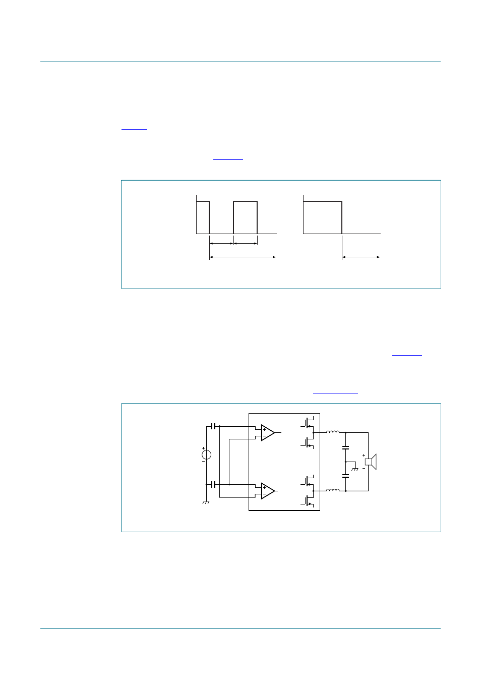
amplifier. The input configuration for a mono BTL application is illustrated in
.
In SE configuration it is also recommended to connect the two differential inputs in
anti-phase. This has advantages for the current handling of the power supply at low signal
frequencies and minimizes supply pumping (see also
).
8.7 Output voltage buffers
When pin POWERUP is set HIGH, the half supply output voltage buffers are switched on
in asymmetrical supply configuration. The start-up will be pop free since the device starts
switching when the capacitor on pin HVPREF and the SE capacitors are completely
charged.
Output voltage buffers:
Fig 6.
Diagnostic output for different short-circuit conditions
001aad759
≈
50 ms
shorted load
amplifier
restart
no restart
≈
50 ms
0 V
2.4 V
V
o
short to
supply line
0 V
2.4 V
V
o
Fig 7.
Input configuration for mono BTL application
001aad760
IN1P
OUT1
audio
input
IN2P
IN2N
IN1N
OUT2
