Circuit description, 2. drive and final amplifier, 3. apc circuit – Kenwood TK-480 User Manual
Page 17
16
TK-480/481
CIRCUIT DESCRIPTION
Fig. 6
Microphone amplifier
Fig. 7
Drive and final amplifier and APC circuit
HPF
ALC
COMP
LPF
HPF
15
16
18
SW
19
DTMF
9
8
IC12
12
LIMIT
MIC
SW
MIC
EXT.
MIC
Q300
D11
6
I5
O5
D/A
IC4
SUM
AMP
IC3 (2/2)
I2
O2
D/A
IC4
AF
MUTE
5R
Q21
I1
O1
D/A
IC4
BUFF
AMP
IC1
IC14
VCO
X2
VCXO
Q301
MSW
PRE EMP
IDC
LSD
MUTE
Q7
Pre-DRIVE
AMP
DRIVE
AMP
Q12
Q11
IC30
RF
POWER AMP
From
T/R SW
(D5)
LPF
ANT
SW
D7
ANT
+B
R127
R128
R129
REF
VOL
(IC4)
IC21
(1/2)
IC21
(2/2)
VDD
VGG
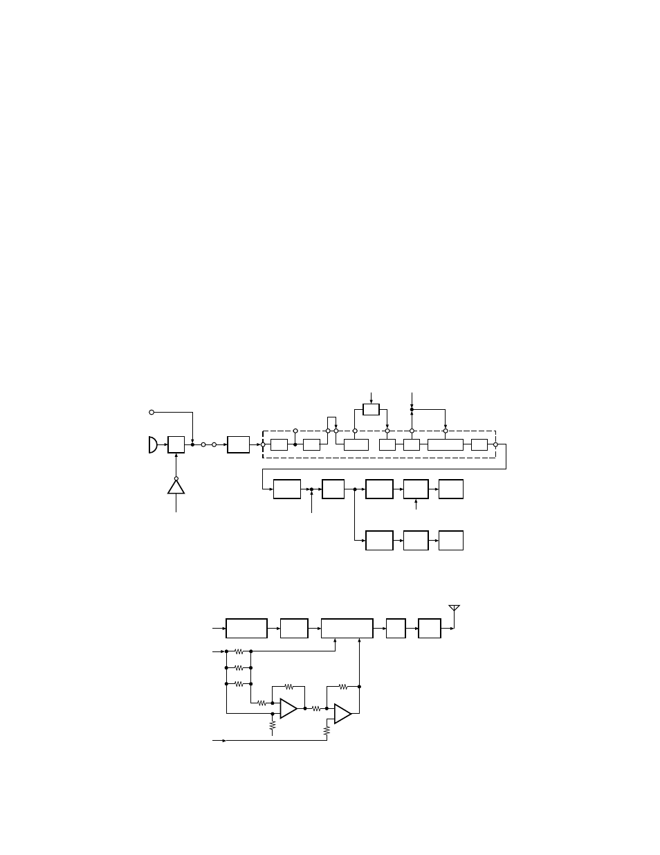
The signal from microphone passes through the limitter
circuit in D11, and through the high-pass filter, the ALC cir-
cuit, the low-pass filter, the high-pass filter, and pre-empha-
sis/IDC circuit in IC12. When encoding DTMF, mute switch
(Q7) is turned OFF for muting the microphone input signal.
The signal passes through the D/A converter (IC4) for the
maximum deviation adjustment, and enters the summing
amplifier consisting of IC3 (2/2), and is mixed with the low
speed data from the CPU (IC15).
The output signal from the summing amplifier passes
through the D/A converter (IC4) again for the TA maximum
deviation adjustment,and the AF switch (Q21 is off in TX),
and goes to the VCO modulation input.
The other output signal from the summing amplifier
passes through the D/A converter (IC4) again for the BAL
adjustment,and the buffer amplifier (IC1 (2/2)), and goes to
the VCXO modulation input.
4-2. Drive and Final amplifier
The signal from the T/R switch (D5 is on) is amplified by
the pre-drive (Q11) and drive amplifier (Q12) to 50mW.
The output of the drive amplifier is amplified by the RF
power amplifier (IC30) to 2.5W (1W when the power is low).
The RF power amplifier consists of two stages MOS FET
transistor. The output of the RF power amplifier is then
passed through the harmonic filter (LPF) and antenna switch
(D7 is on) and applied to the antenna terminal.
4-3. APC circuit
The APC circuit always monitors the current flowing
through the RF power amplifier (IC30) and keeps a constant
current. The voltage drop at R127, R128 and R129 is caused
by the current flowing through the RF power amplifier and
this voltage is applied to the differential amplifier (IC21 1/2).
IC21 (2/2) compares the output voltage of IC21 (1/2) with
the reference voltage from IC4, and the output of IC21 (2/2)
controls the VGG of the RF power amplifier to make the
both voltages to same voltage.
The change of power high/low is carried out by the
change of the reference voltage. Q14,15 and 18 are turned
on in transmit and the APC circuit is active.