True ide read/write access timing, Table 14: true ide read/write access timing – Silicon Image SiliconDrive SSDS00-3650H-R User Manual
Page 24
S
ILICON
S
YSTEMS
P
ROPRIETARY
This document and the information contained within it is confidential and proprietary to SiliconSystems, Inc.
All unauthorized use and/or reproduction is prohibited.
P
AGE
12
J
UNE
17, 2008
D
OCUMENT
: 3650H-02DSR
SSD-H
XXX
(I)-3650 D
ATA
S
HEET
E
LECTRICAL
S
PECIFICATION
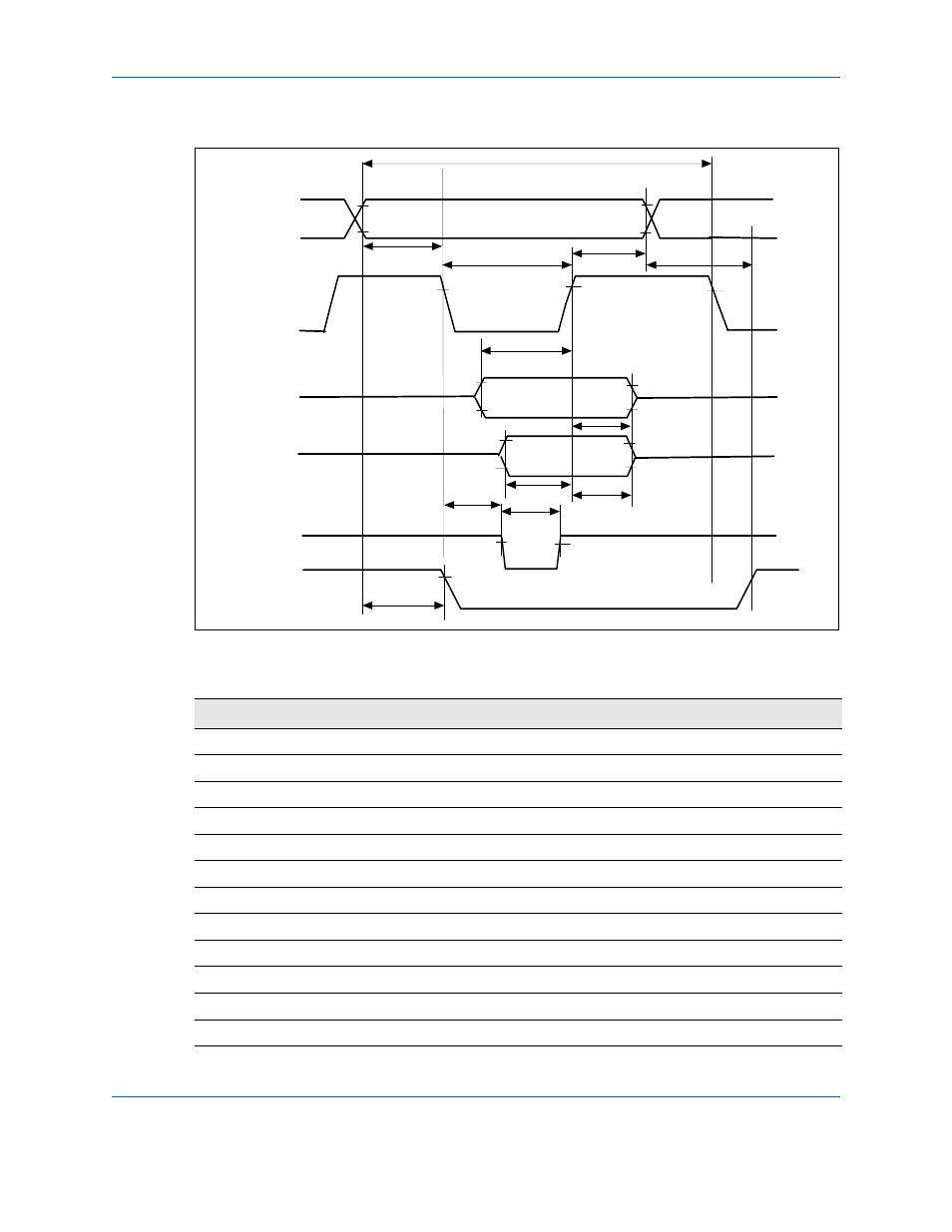
True IDE Read/Write Access Timing
Figure 6: True IDE Read/Write Access Timing Diagram
Note:
(1) IOIS16 and INPACK are not supported.
Table 14: True IDE Read/Write Access Timing
Symbol Parameter
Minimum Maximum Units
t
ICL
Cycle Time
100
-
ns
t
AVRWL
Address Valid to DIOR,DIOW Setup Time
15
-
ns
t
RWPW
DIOR, DIOW Pulse Width
65
-
ns
t
DVWL
DIOW Data Setup Time
20
-
ns
t
DXWH
DIOW Data Hold Time
5
-
ns
t
DVRL
DIOR Data Setup Time
15
-
ns
t
DXRH
DIOR Data Hold Time
5
-
ns
t
AV16L
Address Valid to IOCS16 Assertion
-
(1)
ns
t
AX16H
Address Valid to IOCS16 Negation
-
(1)
ns
t
AXRWH
DIOW,DIOR to Address Valid Hold Time
10
-
ns
t
IOST
IORDY Setup Time
-
(1)
ns
t
IOPW
IORDY Pulse Width
-
(1)
ns
ADDRESS Valid
CS0, CS1, DA[2::0]
____ _____
DIOR,DIOW
WRITE
DD[15::00]
READ
DD[15::00]
IORDY
t
ICL
t
DVWL
t
AVRWL
t
RWPW
t
AXRWH
t
AX16H
t
DXWH
t
DVRL
t
IOST
t
IOPW
t
DXRH
t
AV16L
______
IOIS16