I/o access write timing, Figure 5: i/o access write timing diagram, Table 13: i/o access write timing – Silicon Image SiliconDrive SSDS00-3650H-R User Manual
Page 23
E
LECTRICAL
S
PECIFICATION
SSD-H
XXX
(I)-3650 D
ATA
S
HEET
S
ILICON
S
YSTEMS
P
ROPRIETARY
This document and the information contained within it is confidential and proprietary to SiliconSystems, Inc.
All unauthorized use and/or reproduction is prohibited.
D
OCUMENT
: 3650H-02DSR
J
UNE
17, 2008
P
AGE
11
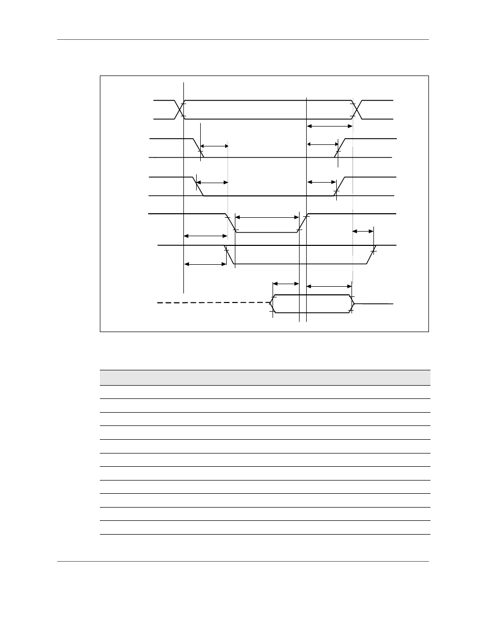
I/O Access Write Timing
Figure 5: I/O Access Write Timing Diagram
Note:
(1) IOIS16 and INPACK are not supported.
Table 13: I/O Access Write Timing
Symbol
Parameter
Minimum
Maximum
Units
t
IGHDX
Data Hold following IOWR
5
-
ns
t
IGHQX
Data Setup before IOWR
20
-
ns
t
IGLIGH
IOWR Pulse Width
65
-
ns
t
AVIGL
Address Setup before IOWR
25
-
ns
t
AXIGH
Address Hold following IOWR
10
-
ns
t
CLIGL
CE Setup before IOWR
5
-
ns
t
CHIGH
CE Hold following IOWR
10
-
ns
t
RLIGL
REG Setup before IOWR
5
-
ns
t
RHIGH
REG Hold following IOWR
0
-
ns
t
AVISL
IOIS16 Delay Falling from Address
-
(1)
ns
t
AXISH
IOIS16 Delay Rising from Address
-
(1)
ns
A[10::0]
____
REG
__
CE
_____
IOWR
______
IOIS16
t
RLIGL
t
AXIGH
D[15::0]
t
CLIGL
t
CHIGH
t
RHIGH
t
IGLIGH
t
AXISH
t
AVISL
t
AVIGL
t
IGHQX
t
IGHDX