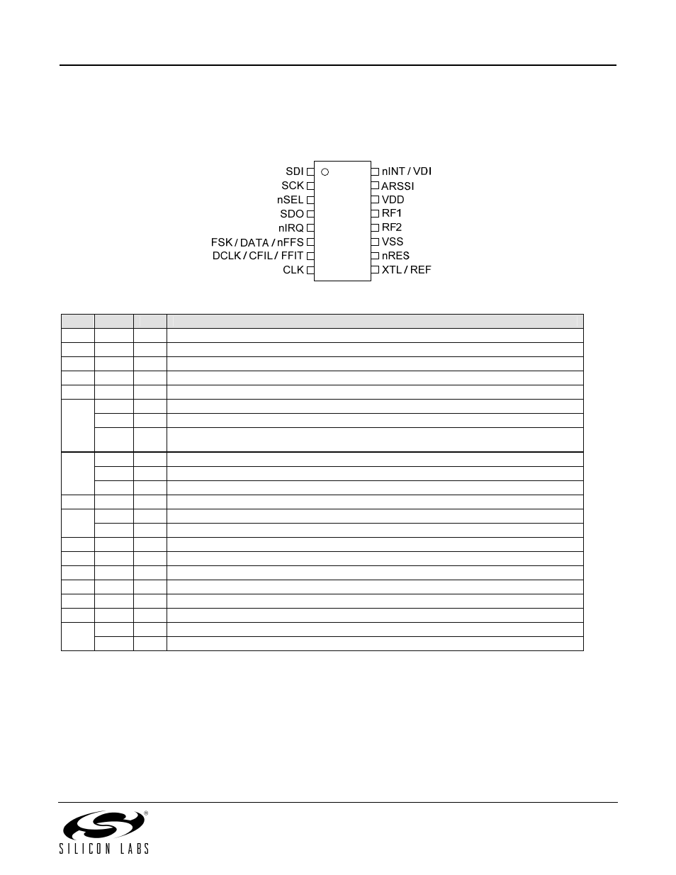
Si4421 package pin definitions – Silicon Laboratories SI4421 User Manual
Page 4
Si4421
PACKAGE PIN DEFINITIONS
Pin type key: D=digital, A=analog, S=supply, I=input, O=output, IO=input/output
Pin
Name
Type
Function
1
SDI
DI
Data input of the serial control interface
2
SCK
DI
Clock input of the serial control interface
3
nSEL
DI
Chip select input of the serial control interface (active low)
4
SDO
DO
Serial data output with bus hold
5
nIRQ
DO
Interrupt request output (active low)
FSK
DI
Transmit FSK data input (internal pull up resistor 133 k)
DATA
DO
Received data output (FIFO not used)
6
nFFS DI
FIFO select input (active low). In FIFO mode, when bit ef is set in Configuration Setting Command,
page 15 (internal pull up resistor 133 k)
DLCK
DO
Received data clock output (Digital filter used, FIFO not used)
CFIL
AIO
External data filter capacitor connection (Analog filter used)
7
FFIT
DO
FIFO interrupt (active high). In FIFO mode, when bit ef is set in Configuration Setting Command
8
CLK
DO
Microcontroller clock output
XTL
AIO
Crystal connection (the other terminal of crystal to VSS) or external reference input
9
REF
AIO
External reference input. Use 33 pF series coupling capacitor
10
nRES
DIO
Open drain reset output with internal pull-up and input buffer (active low)
11
VSS
S
Ground reference voltage
12
RF2
AIO
RF differential signal input/output
13
RF1
AIO
RF differential signal input/output
14
VDD
S
Positive supply voltage
15
ARSSI
AO
Analog RSSI output
nINT
DI
Interrupt input (active low)
16
VDI
DO
Valid data indicator output
Note: The actual mode of the multipurpose pins (pin 6 and 7) is determined by the TX/RX data I/O settings of the transceiver.
4