Cc77h, B8aah, Si4421 – Silicon Laboratories SI4421 User Manual
Page 24: Pll setting command, Transmitter register write command
Si4421
12. PLL Setting Command
Bit
15 14 13 12 11 10 9 8 7 6 5 4 3 2 1 0
POR
1 1 0 0 1 1 0 0 0
ob1
ob0
1 dly
ddit
1
bw0 CC77h
Bits 6-5 (ob1-ob0):
Microcontroller output clock buffer rise and fall time control. The ob1-ob0 bits are changing the output drive
current of the CLK pin. Higher current provides faster rise and fall times but can cause interference.
ob1
ob0
Selected µC CLK frequency
1
1
5 or 10 MHz (recommended)
1 0
3.3
MHz
0
X
2.5 MHz or less
Note: Needed for optimization of the RF performance. Optimal settings can vary according to the external load capacitance.
Bit 3 (dly): Switches on the delay in the phase detector when this bit is set.
Bit 2 (ddit): When set, disables the dithering in the PLL loop.
Bit 0 (bw0):
PLL bandwidth can be set for optimal TX RF performance.
bw0
Max bit rate [kbps]
Phase noise at 1MHz offset [dBc/Hz]
0 86.2
-107
1 256
-102
Note: POR default settings of the register were carefully selected to cover almost all typical applications. When changing these
values, examine thoroughly the output RF spectrum. For more information, contact Silicon Labs Support.
13. Transmitter Register Write Command
Bit
15 14 13 12 11 10 9 8 7 6 5 4 3 2 1 0
POR
1 0 1 1 1 0 0 0 t7 t6 t5 t4 t3 t2 t1 t0
B8AAh
With this command, the controller can write 8 bits (t7 to t0) to the transmitter data register. Bit 7 (el) must be set in Configuration
Setting Command (page 15).
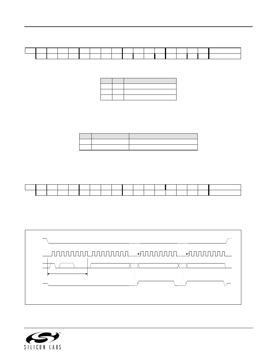
Multiple Byte Write with Transmit Register Write Command:
nSEL
SCK
SDI
SDO
TX BYTE1
TX BYTEn
TX BYTE2
command
T r a n s m i t R e g i s t e r W r i t e
(REGISTER IT
in TX mode*)
Note: *The transceiver is in transmit (TX) mode when bit er is cleared using the Power Management Command
Note: Alternately the transmit register can be directly accessed by nFFS (pin6).
24