3 system and power management signals – Intel GD82559ER User Manual
Page 15
Datasheet
9
Networking Silicon —GD82559ER
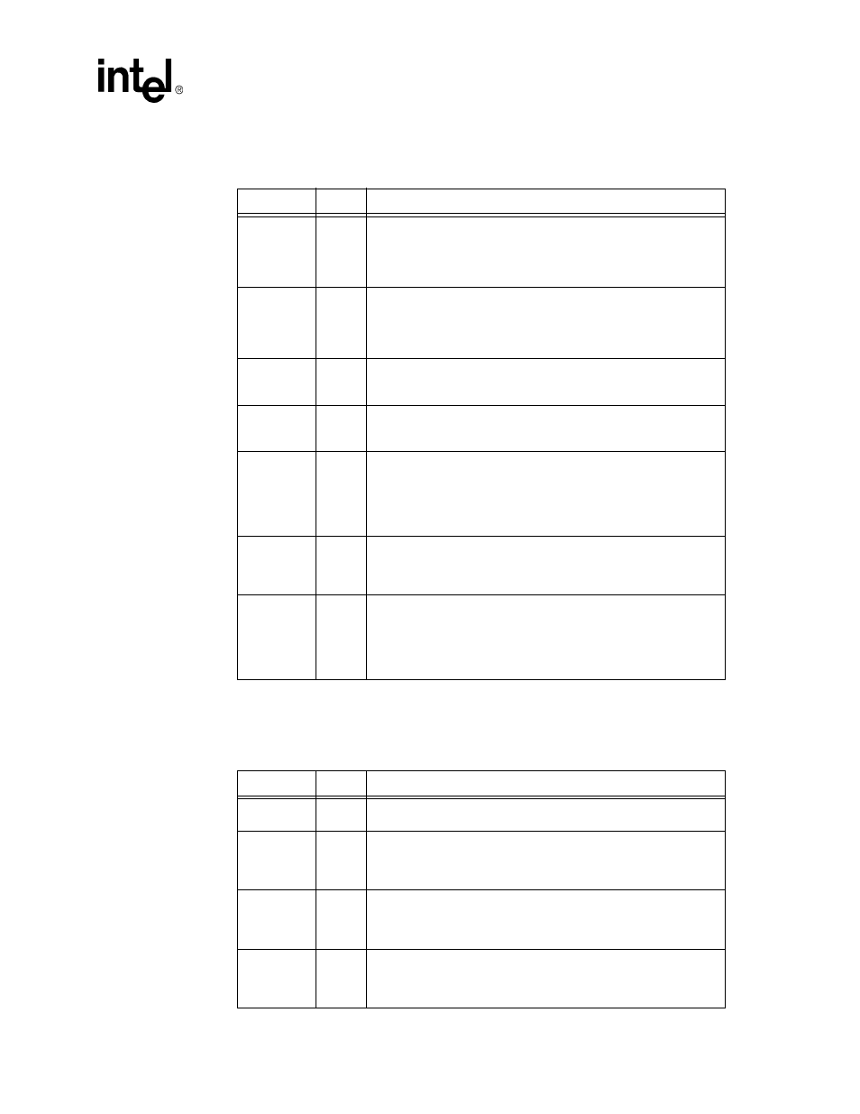
3.2.3
System and Power Management Signals
3.3
Local Memory Interface Signals
Symbol
Type
Name and Function
CLK
IN
Clock. The Clock signal provides the timing for all PCI transactions
and is an input signal to every PCI device. The 82559ER requires a
PCI Clock signal (frequency greater than or equal to 16 MHz) for
nominal operation. The 82559ER supports Clock signal suspension
using the Clockrun protocol.
CLKRUN#
IN/OUT
O/D
Clockrun. The Clockrun signal is used by the system to pause or slow
down the PCI Clock signal. It is used by the 82559ER to enable or
disable suspension of the PCI Clock signal or restart of the PCI clock.
When the Clockrun signal is not used, this pin should be connected to
an external pull-down resistor.
RST#
IN
Reset. The PCI Reset signal is used to place PCI registers,
sequencers, and signals into a consistent state. When RST# is
asserted, all PCI output signals will be tri-stated.
PME#
O/D
Power Management Event. The Power Management Event signal
indicates that a power management event has occurred in a PCI bus
system.
ISOLATE#
IN
Isolate. The Isolate signal is used to isolate the 82559ER from the
PCI bus. When Isolate is active (low), the 82559ER does not drive its
PCI outputs (except PME#) or sample its PCI inputs (including CLK
and RST#). If the 82559ER is not powered by an auxiliary power
source, the ISOLATE# pin should be pulled high to the bus Vcc
through a 4.7K-62K resistor.
ALTRST#
IN
Alternate Reset. The Alternate Reset signal is used to reset the
82559ER on power-up. In systems that support an auxiliary power
supply, ALTRST# should be connected to a power-up detection circuit.
Otherwise, ALTRST# should be tied to V
cc
.
VIO
B
IN
Voltage Input/Output. The VIO pin is the a voltage bias pin for the
PCI interface. This pin should be connected to 5V ± 5% in a 5 volt PCI
system and 3.3 volts in a 3.3 volt PCI system. Be sure to install a 10K
pull-up resistor. This resistor acts as a current limit resistor in system
where the VIO bias voltage maybe shutdown. In this cases the
82559ER may consume additional current without a resistor.
Symbol
Type
Name and Function
FLD[7:0]
T/S
Flash Data Input/Output. These pins are used for Flash data
interface.
FLA[16]/
CLK25
OUT
Flash Address[16]/25 MHz Clock. This multiplexed pin is controlled
by the status of the Flash Address[7] (FLA[7]) pin. If FLA[7] is left
floating, this pin is used as FLA[16]; otherwise, if FLA[7] is connected
to a pull-up resistor, this pin is used as a 25 MHz clock.
FLA[15]/
EESK
OUT
Flash Address[15]/EEPROM Data Output. During Flash accesses,
this multiplexed pin acts as the Flash Address [15] output signal.
During EEPROM accesses, it acts as the serial shift clock output to
the EEPROM.
FLA[14]/
EEDO
IN/OUT
Flash Address[14]/EEPROM Data Output. During Flash accesses,
this multiplexed pin acts as the Flash Address [14] output signal.
During EEPROM accesses, it acts as serial input data to the EEPROM
Data Output signal.