Bios ep-8kta, 3 advanced chipset features – IBM EP-8KTA User Manual
Page 34
BIOS
EP-8KTA
Page 4-8
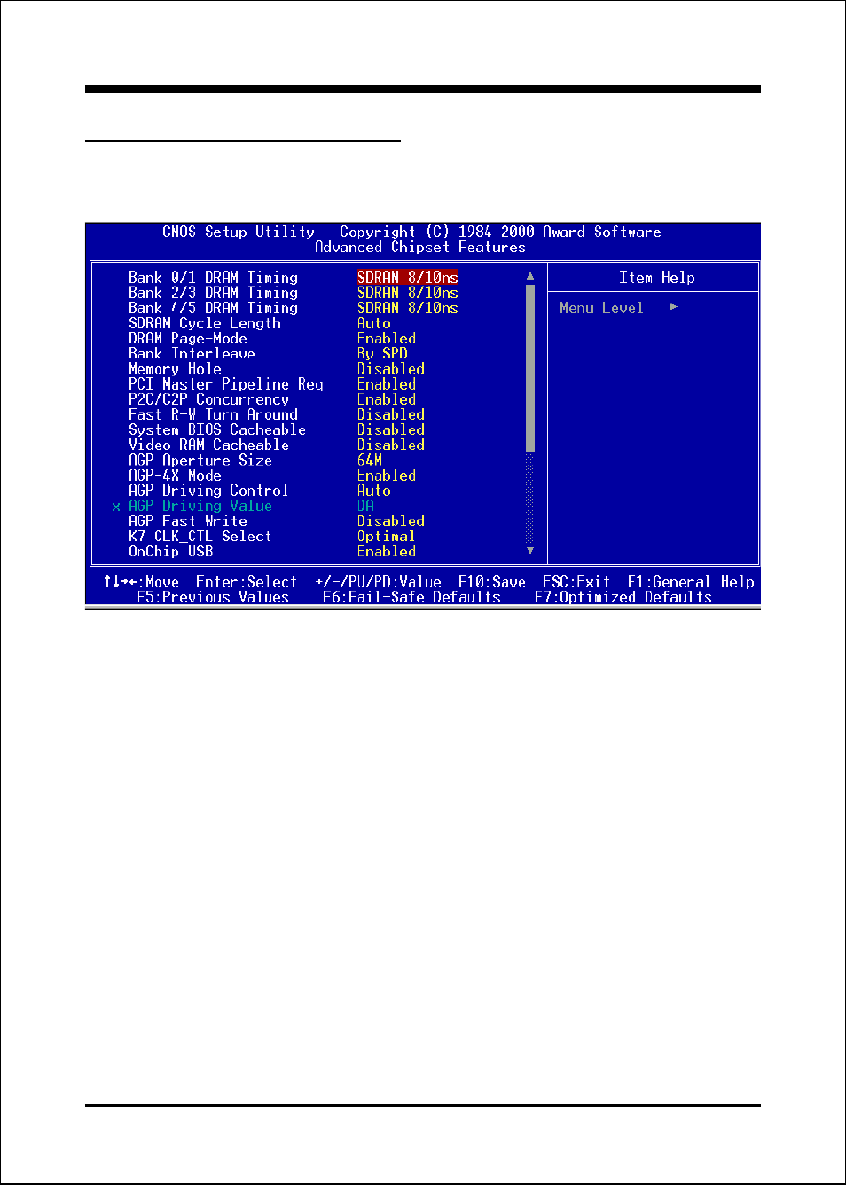
Bank 0/1, 2/3, 4/5 DRAM Timing: This value in this field is set by the system
board manufacturer, depending on whether the board has paged DRAMs or EDO
(extended data output) DRAMs.
The Choice: Bank 0/1, 2/3, 4/5.
SDRAM Cycle length: This setting defines the CAS timing parameter of the
SDRAM in terms of clocks. The default is 3.
2: Provides faster memory performance.
3: Provides better memory compatibility.
Auto: Determined by BIOS.
Bank Interleave: The item allows you to set how many banks of SDRAM support
in your mainboard.
The Choice: 2 Bank, 4 Bank, Disabled.
DRAM Page-Mode: The item will active or inactive chipset page registers.
Enabled: Page-Mode Enabled.
Disabled: No page registers update and non Page-Mode operation.
4-3 Advanced Chipset Features
Choose the CHIPSET FEATURES SETUP in the CMOS SETUP UTILITY menu
to display following menu.
Figure 4: Chipset Features Setup
- ADSL Bridge/ Router Heritage (167 pages)
- 27L2579 (20 pages)
- DR550 (128 pages)
- LCD/LVDS/LAN (154 pages)
- 22P6959 (50 pages)
- ThinkPad 73P3315 (62 pages)
- ULTRABAY 2000 (62 pages)
- SYSTEM STORAGE DS4000 (38 pages)
- uPD78P083 (274 pages)
- 2257 (252 pages)
- 51 (248 pages)
- 2 (72 pages)
- System Storage N6040 (6 pages)
- 22P6960 (56 pages)
- 07N4108 (11 pages)
- 22P9176 (76 pages)
- 22P6972 (46 pages)
- 48X (60 pages)
- 22P6979 (52 pages)
- 8313 (314 pages)
- 19K4543 (56 pages)
- SC30-3865-04 (513 pages)
- DTLA-305020 (2 pages)
- WebSphere Adapters (226 pages)
- x Series 200 (152 pages)
- Storage Device Enclosure 7214 (4 pages)
- Tivoli and Cisco (516 pages)
- ZSERIES 890 (12 pages)
- 10K0001 (20 pages)
- 31P8128 (112 pages)
- 09N4076 (78 pages)
- Computer Drive (44 pages)
- N7000 (8 pages)
- All-in-One Super7 Single Board Computer PCM-5896 (128 pages)
- 20X (17 pages)
- 73P3309 (64 pages)
- W2H (68 pages)
- 22P6415 (62 pages)
- THINKCENTER 8187 (290 pages)
- NETVISTA 6830/6831 (152 pages)
- 802.11g Wireless Broadband Router WRT-410 (69 pages)
- THINKPAD 72 W DC (70 pages)
- ThinkPad 73P3279 (54 pages)
- HS64 (13 pages)
- THINKVISION MONITOR L150P (35 pages)