Intel UPI-C42 User Manual
Page 2
UPI-C42 UPI-L42
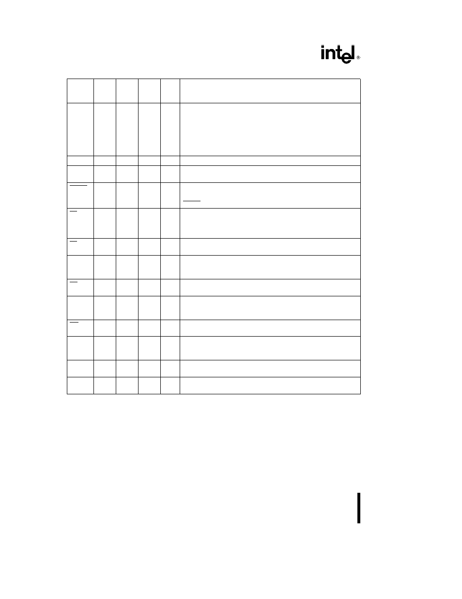
Table 1 Pin Description
DIP
PLCC
QFP
Symbol
Pin
Pin
Pin
Type
Name and Function
No
No
No
TEST 0
1
2
18
I
TEST INPUTS
Input pins which can be directly tested using conditional
branch instructions
TEST 1
39
43
16
FREQUENCY REFERENCE
TEST 1 (T
1
) functions as the event timer
input (under software control) TEST 0 (T
0
) is a multi-function pin used
during PROM programming and ROM EPROM verification during Sync
Mode to reset the instruction state to S1 and synchronize the internal clock
to PH1
XTAL 1
2
3
19
O
OUTPUT
Output from the oscillator amplifier
XTAL 2
3
4
20
I
INPUT
Input to the oscillator amplifier and internal clock generator
circuits
RESET
4
5
22
I
RESET
Input used to reset status flip-flops set the program counter to
zero and force the UPI-C42 from the suspend power down mode
RESET is also used during EPROM programming and verification
SS
5
6
23
I
SINGLE STEP
Single step input used in conjunction with the SYNC output
to step the program through each instruction (EPROM) This should be tied
to a5V when not used This pin is also used to put the device in Sync
Mode by applying 12 5V to it
CS
6
7
24
I
CHIP SELECT
Chip select input used to select one UPI microcomputer
out of several connected to a common data bus
EA
7
8
25
I
EXTERNAL ACCESS
External access input which allows emulation
testing and ROM EPROM verification This pin should be tied low if
unused
RD
8
9
26
I
READ
I O read input which enables the master CPU to read data and
status words from the OUTPUT DATA BUS BUFFER or status register
A
0
9
10
27
I
COMMAND DATA SELECT
Address Input used by the master processor
to indicate whether byte transfer is data (A
0
e
0 F1 is reset) or command
(A
0
e
1 F1 is set) A
0
e
0 during program and verify operations
WR
10
11
28
I
WRITE
I O write input which enables the master CPU to write data and
command words to the UPI INPUT DATA BUS BUFFER
SYNC
11
13
29
O
OUTPUT CLOCK
Output signal which occurs once per UPI instruction
cycle SYNC can be used as a strobe for external circuitry it is also used to
synchronize single step operation
D
0
– D
7
(BUS)
12 – 19
14 – 21
30 – 37
I O
DATA BUS
Three-state bidirectional DATA BUS BUFFER lines used to
interface the UPI microcomputer to an 8-bit master system data bus
P
10
– P
17
27 – 34
30 – 33
2 – 10
I O
PORT 1
8-bit PORT 1 quasi-bidirectional I O lines P
10
– P
17
access the
signature row and security bit
35 – 38
2