B.3 output loads, Chip power-up and lvi/lvr graphical explanation, Output loads – Motorola MC9S12GC-Family User Manual
Page 96: B.3.1, Resistive loads, Figure b-1, B.3.1 resistive loads
Device User Guide — 9S12C128DGV1/D V01.05
96
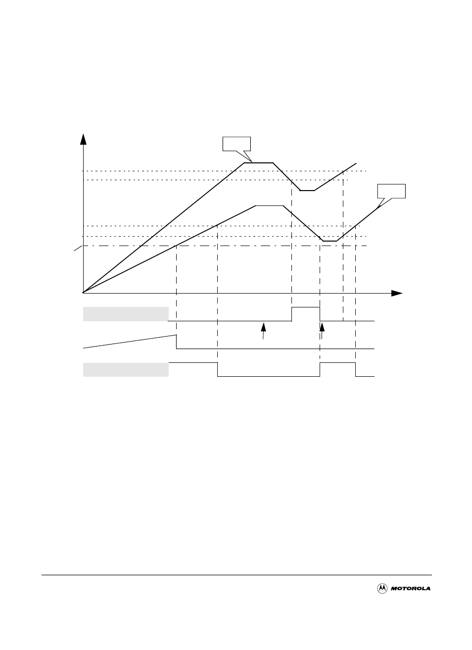
B.2 Chip Power-up and LVI/LVR graphical explanation
Voltage regulator sub modules LVI (low voltage interrupt), POR (power-on reset) and LVR (low voltage
reset) handle chip power-up or drops of the supply voltage. Their function is described in
Figure B-1 Voltage Regulator - Chip Power-up and Voltage Drops (not scaled)
B.3 Output Loads
B.3.1 Resistive Loads
The on-chip voltage regulator is intended to supply the internal logic and oscillator circuits allows no
external DC loads.
V
LVID
V
LVIA
V
LVRD
V
LVRA
V
PORD
LVI
POR
LVR
t
V
V
DDA
V
DD
LVI enabled
LVI disabled due to LVR
This manual is related to the following products: