Figure 3-1 clock connections, Section 4 modes of operation, 1 overview – Motorola MC9S12GC-Family User Manual
Page 65: 2 chip configuration summary, Overview, Chip configuration summary, Figure 3-1, Clock connections
Device User Guide — 9S12C128DGV1/D V01.05
65
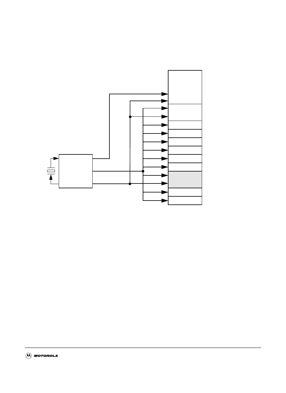
The Clock and Reset Generator provides the internal clock signals for the core and all peripheral modules.
shows the clock connections from the CRG to all modules. Consult the CRG Block User
Guide for details on clock generation.
Figure 3-1 Clock Connections
Section 4 Modes of Operation
4.1 Overview
Eight possible modes determine the operating configuration of the MC9S12C Family. Each mode has an
associated default memory map and external bus configuration controlled by a further pin.
Three low power modes exist for the device.
4.2 Chip Configuration Summary
The operating mode out of reset is determined by the states of the MODC, MODB, and MODA pins during
reset. The MODC, MODB, and MODA bits in the MODE register show the current operating mode and
provide limited mode switching during operation. The states of the MODC, MODB, and MODA pins are
CRG
bus clock
core clock
EXTAL
XTAL
oscillator clock
S12_CORE
VREG
RAM
SCI
ATD
Flash
TIM
TPM
SPI
MSCAN
PIM
Not on 9S12GC