Table a-1 absolute maximum ratings, A.1.5, Absolute maximum ratings – Motorola MC9S12GC-Family User Manual
Page 85: Table a-1, A.1.5 absolute maximum ratings, Or v
Device User Guide — 9S12C128DGV1/D V01.05
85
A.1.5 Absolute Maximum Ratings
Absolute maximum ratings are stress ratings only. A functional operation under or outside those maxima
is not guaranteed. Stress beyond those limits may affect the reliability or cause permanent damage of the
device.
This device contains circuitry protecting against damage due to high static voltage or electrical fields;
however, it is advised that normal precautions be taken to avoid application of any voltages higher than
maximum-rated voltages to this high-impedance circuit. Reliability of operation is enhanced if unused
inputs are tied to an appropriate logic voltage level (e.g., either V
SS5
or V
DD5
).
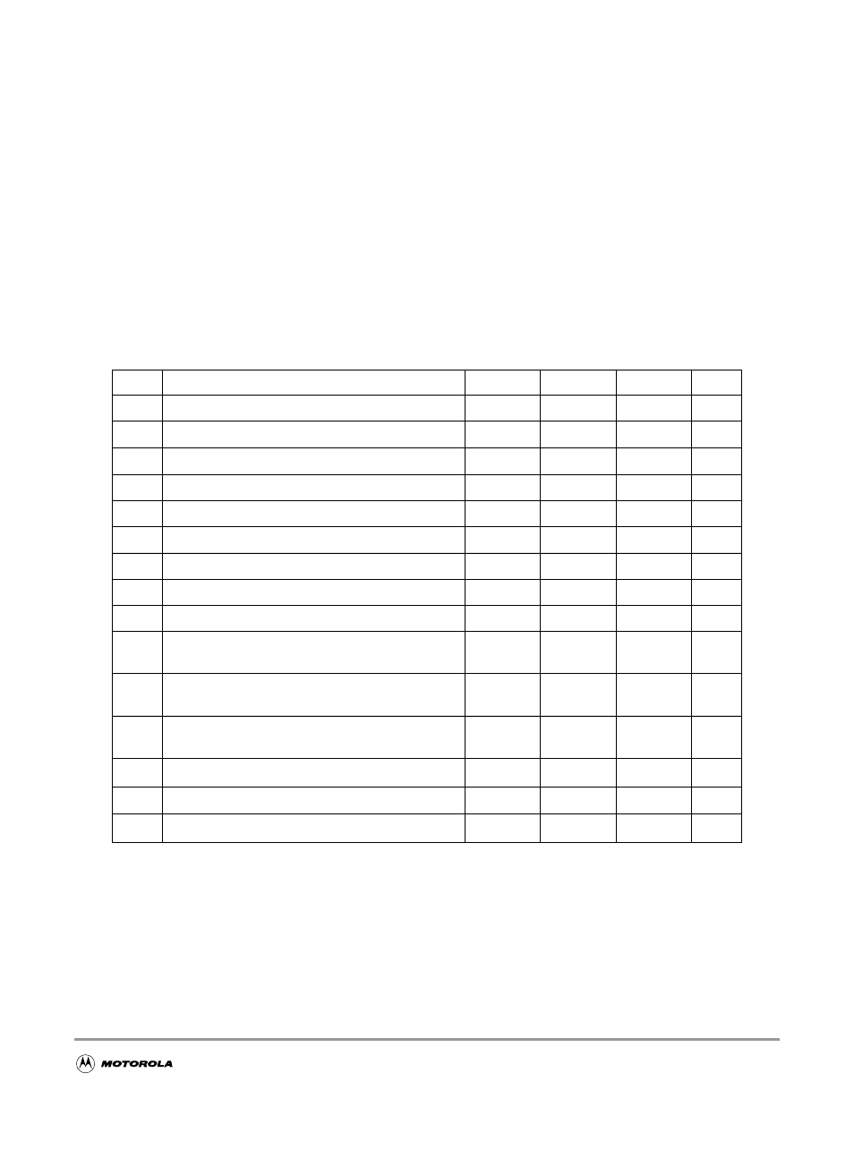
Table A-1 Absolute Maximum Ratings
Num
Rating
Symbol
Min
Max
Unit
1
I/O, Regulator and Analog Supply Voltage
V
DD5
-0.3
6.5
V
2
Digital Logic Supply Voltage
1
NOTES
:
1. The device contains an internal voltage regulator to generate the logic and PLL supply out of the I/O supply.
The absolute maximum ratings apply when the device is powered from an external source.
V
DD
-0.3
3.0
V
3
PLL Supply Voltage
V
DDPLL
-0.3
3.0
V
4
Voltage difference VDDX to VDDR and VDDA
∆
VDDX
-0.3
0.3
V
5
Voltage difference VSSX to VSSR and VSSA
∆
VSSX
-0.3
0.3
V
6
Digital I/O Input Voltage
V
IN
-0.3
6.5
V
7
Analog Reference
V
RH,
V
RL
-0.3
6.5
V
8
XFC, EXTAL, XTAL inputs
V
ILV
-0.3
3.0
V
9
TEST input
V
TEST
-0.3
10.0
V
10
Instantaneous Maximum Current
Single pin limit for all digital I/O pins
2
2. All digital I/O pins are internally clamped to V
SSX
and V
DDX
, V
SSR
and V
DDR
or V
SSA
and V
DDA
.
I
D
-25
+25
mA
11
Instantaneous Maximum Current
Single pin limit for XFC, EXTAL, XTAL
3
3. These pins are internally clamped to V
SSPLL
and V
DDPLL
I
DL
-25
+25
mA
12
Instantaneous Maximum Current
Single pin limit for TEST
4
4. This pin is clamped low to V
SSX
, but not clamped high. This pin must be tied low in applications.
I
DT
-0.25
0
mA
13
Operating Temperature Range (packaged)
T
A
– 40
125
°
C
14
Operating Temperature Range (junction)
T
J
– 40
140
°
C
15
Storage Temperature Range
T
stg
– 65
155
°
C