Section 3 system clock description, Vdda, vssa — power supply pins for atd and vreg, Vrh, vrl — atd reference voltage input pins – Motorola MC9S12GC-Family User Manual
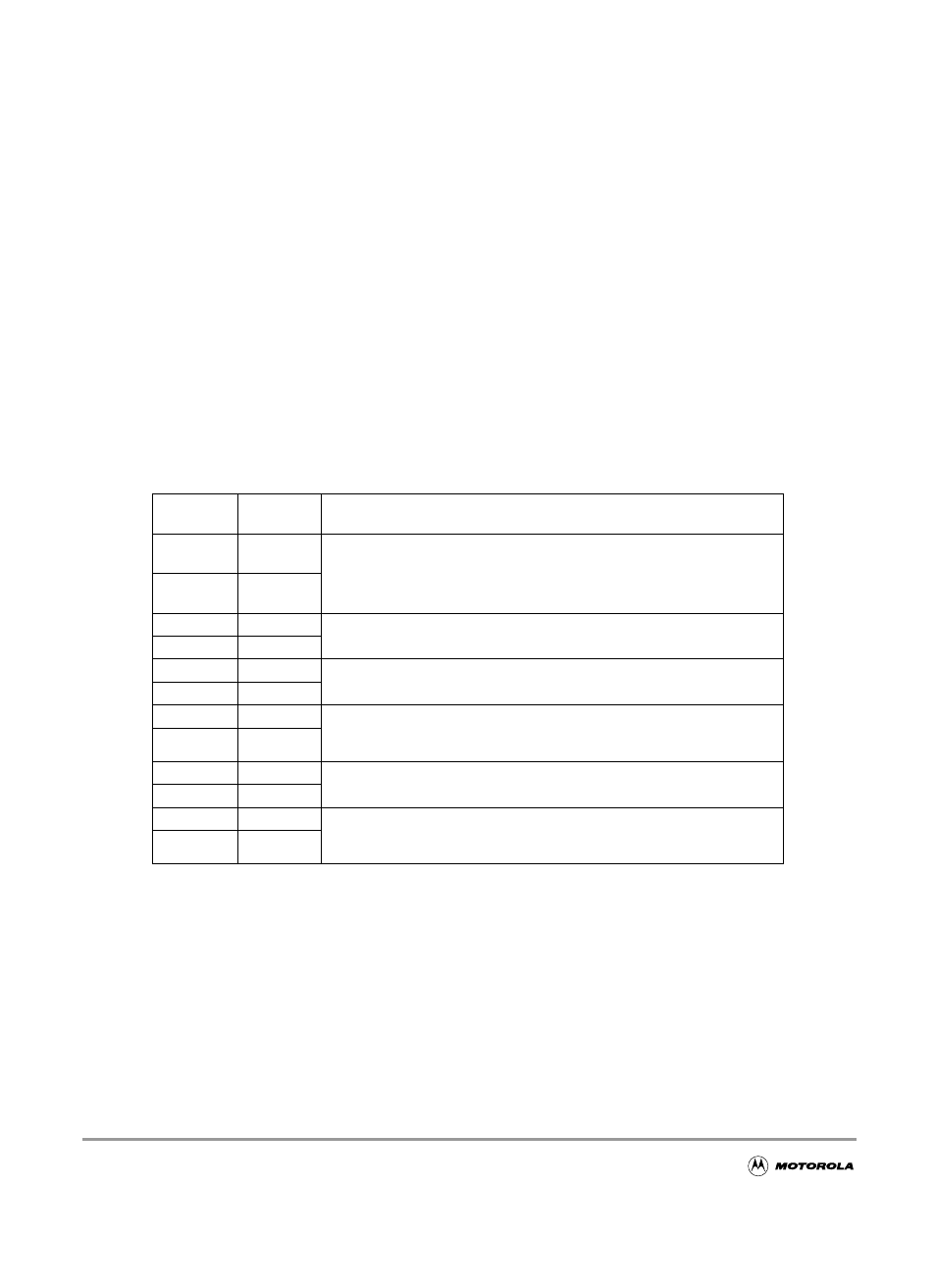
Page 64: Vddpll, vsspll — power supply pins for pll, Table 2-2, Mc9s12c-family power and ground connection summary, 4 vdda, vssa — power supply pins for atd and vreg, 5 vrh, vrl — atd reference voltage input pins, 6 vddpll, vsspll — power supply pins for pll
 Section 3 system clock description, Vdda, vssa — power supply pins for atd and vreg, Vrh, vrl — atd reference voltage input pins | Vddpll, vsspll — power supply pins for pll, Table 2-2, Mc9s12c-family power and ground connection summary, 4 vdda, vssa — power supply pins for atd and vreg, 5 vrh, vrl — atd reference voltage input pins, 6 vddpll, vsspll — power supply pins for pll | Motorola MC9S12GC-Family User Manual | Page 64 / 136
 This manual is related to the following products: