Electrical characteristics – FUJITSU MB91401 User Manual
Page 47
MB91401
47
■
■
■
■
ELECTRICAL CHARACTERISTICS
1.
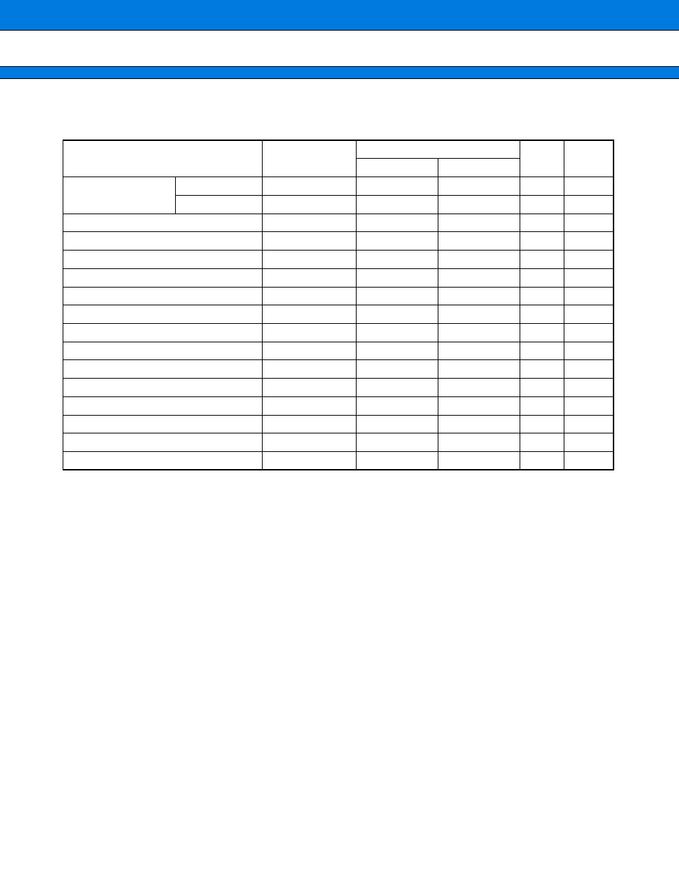
Absolute Maximum Ratings
*1 : This parameter is based on VSS
=
PLLVSS
=
0 V.
*2 : Note that analog power supply voltage and input voltage do not exceed VDDE
+
0.3 V at power on.
*3 : The maximum output current is the peak value for a single pin.
*4 : The average output current is the average current for a single pin over a period of 100 ms.
*5 : The total average output current is the average current for all pins over a period of 100 ms.
WARNING: Semiconductor devices can be permanently damaged by application of stress (voltage, current,
temperature, etc.) in excess of absolute maximum ratings. Do not exceed these ratings.
Notes :
•
Apply equal potential to all of the VDDE pins.
•
Apply equal potential to all of the VDDI pins.
•
Fix all of the VSS pins at 0 V.
•
Leave N.C. pins open.
Parameter
Symbol
Rating
Unit
Remarks
Min
Max
Power supply
voltage*
1
I/O
V
DDE
VSS
−
0.3
VSS
+
4.0
V
Internal
V
DDI
VSS
−
0.3
VSS
+
2.5
V
Analog power supply voltage
PLLVDD
VSS
−
0.3
VSS
+
4.0
V
*2
Input voltage*
1
V
I
VSS
−
0.3
VDDE
+
0.3
V
Output voltage*
1
V
O
VSS
−
0.3
VDDE
+
0.3
V
“L” level maximum output current
I
OL
T.B.D
mA
*3
“L” level average output current
I
OLAV
T.B.D
mA
*4
“L” level total maximum output current
Σ
I
OL
T.B.D
mA
“L” level total average output cur rent
Σ
I
OLAV
T.B.D
mA
*5
“H” level maximum output current
I
OH
T.B.D
mA
*3
“H” level average output current
I
OHAV
T.B.D
mA
*4
“H” level total maximum output current
Σ
I
OH
T.B.D
mA
“H” level total average output cur rent
Σ
I
OHAV
T.B.D
mA
*5
Power consumption
P
D
T.B.D
mW
Operating temperature
Ta
−
10
70
°
C
Storage temperature
Tstg
−
55
150
°
C
Prelminary
2004.11.12