FUJITSU MB91401 User Manual
Page 13
MB91401
13
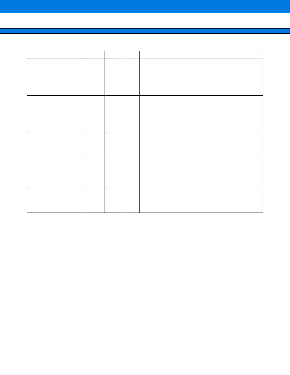
USB IF (5 pin)
Pin name
Pin no.
Polarity
I/O
Circuit
Function/application
UDP
61
I/O
C
USB data D
+
(differential) pin
I/O signal pin on the plus side of the USB data.
Use the LSI with 25
Ω
to 30
Ω
(27
Ω
recommended)
external series load resistors, 1.5 k
Ω
pull-up resistors and
about 100 k
Ω
resistors. Input “0” when the USB macro is
unused.
UDM
183
I/O
C
USB data D
−
(differential) pin
I/O signal pin on the minus side of the USB data.
Use the LSI with 25
Ω
to 30
Ω
(27
Ω
recommended)
external series load resistors, 1.5 k
Ω
pull-up resistors and
about 100 k
Ω
resistors. Input “0” when the USB macro is
unused.
USBINS
182
IN
D
USB insert input pin
USB socket input detection pin. Be sure to input “0” when
not using USB macro.
UCLK48
6
IN
D
48 MHz input (external clock input) pin
This pin inputs an external 48-MHz clock signal.
The USB macro operates based on this clock. Input the
clock with high accuracy (as not only LSI but also a device)
more than 2500 ppm. Input “0” when the USB macro is un-
used.
UCLKSEL
124
IN
D
USB clock select pin
Clock select pin using for USB macro
“0” : Using internal clock
“1” : Using UCLK48
Prelminary
2004.11.12