Applications information, Table 2. interface truth table – Rainbow Electronics MAX547 User Manual
Page 9
_______________________________________________________________________________________
9
__________Applications Information
Multiplying Operation
The MAX547 can be used for multiplying applications.
Its reference accepts both DC and AC signals. The volt-
age at each REF_ input sets the full-scale output voltage
for its respective DACs. Since the reference inputs
accept only positive voltages, multiplying operation is
limited to two quadrants. Do not bypass the reference
inputs when applying AC signals to them. Refer to the
graphs in the
Typical Operating Characteristics
for
dynamic performance of the DACs and output buffers.
Digital Code and Analog Output Voltage
The MAX547 uses offset binary coding. A 13-bit twos-
complement code can be converted to a 13-bit offset
binary code by adding 2
12
= 4096.
Bipolar Output Voltage Range (AGND_ = 0V)
For symmetrical bipolar operation, tie AGND_ to the
system ground. Table 3 shows the relationship between
digital code and output voltage. The following para-
graphs give a detailed explanation of this mode.
The DAC ladder output voltage (V
DAC
) is multiplied by
2 and level shifted by the reference voltage, which is
internally connected to the output amplifiers (Figure 1).
Since the feedback resistors are the same size, the
amplifier’s output voltage is 2 times the voltage at its
noninverting input, minus the reference voltage.
where V
DAC
is the voltage at the amplifier’s noninvert-
ing input (DAC ladder output voltage), and REF_ is the
voltage applied to the reference input of the DAC.
With AGND_ connected to the system ground, the DAC
ladder output voltage is:
where D is the numeric value of the DAC’s binary input
code and n is the DAC’s resolution (13 bits). Replace
V
DAC
in the equation and calculate the output voltage.
D ranges from 0 (2
0
) to 8191 (2
13
- 1).
1LSB
REF–
1
4096
=
VOUT_
2
D
2
REF– REF–
= REF–
D
2
– 1
REF–
D
4096
– 1
13
12
=
(
)
−
=
V
D
2
(REF–)
D
2
(REF–)
DAC
n
13
=
=
VOUT 2(V
)
REF–
DAC
=
−
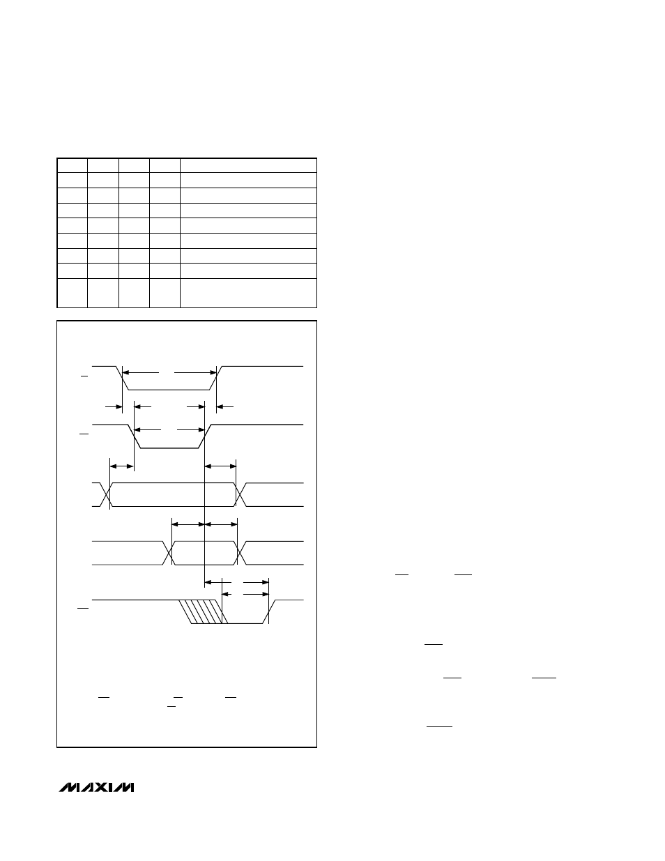
Table 2. Interface Truth Table
MAX547
Octal, 13-Bit Voltage-Output
DAC with Parallel Interface
–
C
—
L
—
R
–
FUNCTION
1
Both latches transparent
1
Both latches latched
1
Both latches latched
–
L
—
D
—
–
–
0
1
1
1
Input latch transparent
1
Input latch latched
1
Input latch latched
X
X
X
–
W
—
R
–
0
0
1
X
–
C
—
S
–
0
1
X
1
X
0
X
1
X
0
All input and DAC latches at
1000hex, outputs at AGND–
X
X
X
1
DAC latch transparent
X
0
CS
WR
A0–A2
D0–D12
LD–
NOTES:
1. ALL INPUT RISE AND FALL TIMES MEASURED FROM 10% TO 90% OF
+5V. t
r
= t
f
= 5ns.
2. MEASUREMENT REFERENCE LEVEL IS
(V
INH
+ V
INL
)/2.
3. IF LD– IS ACTIVATED WHILE WR IS LOW THEN LD– MUST STAY LOW
FOR t3 OR LONGER AFTER WR GOES HIGH.
t
1
t
2
t
9
t
10
t
7
t
8
t
5
t
6
t
3
t
3
Figure 3. Write-Cycle Timing